
Instruction Manual

MAX1198
Dual, 8-Bit, 100Msps, 3.3V, Low-Power ADC
with Internal Reference and Parallel Outputs
_______________________________________________________________________________________ 5
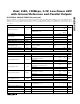
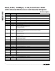
PARAMETER SYMBOL CONDITIONS MIN T YP MAX UNITS
CLK
0.2 ×
V
DD
Input Low Threshold V
IL
PD, OE, SLEEP, T/B
0.2 ×
OV
DD
V
Input Hysteresis V
HYST
0.15 V
I
IH
V
IH
= V
DD
= OV
DD
±20
Input Leakage
I
IL
V
IL
= 0 ±20
µA
Input Capacitance C
IN
5pF
DIGITAL OUTPUTS ( D7A–D0A, D7B–D0B)
Output Voltage Low V
OL
I
SINK
= -200µA 0.2 V
Output Voltage High V
OH
I
SOURCE
= 200µA
OV
DD
-
0.2
V
Three-State Leakage Current I
LEAK
OE = OV
DD
±10 µA
Three-State Output Capacitance C
OUT
OE = OV
DD
5pF
POWER REQUIREMENTS
Analog Supply Voltage Range V
DD
2.7 3.3 3.6 V
Output Supply Voltage Range OV
DD
C
L
= 15pF 1.7 2.5 3.6 V
Operating, f
INA & B
= 20MHz at -1dB FS
applied to both channels
80 95
Sleep mode 3.2
mA
Analog Supply Current I
VDD
Shutdown, clock idle, PD = OE = OV
DD
0.15 20 µA
Operating, f
INA & B
= 20MHz at -1dB FS
applied to both channels (Note 6)
11.5 mA
Sleep mode 2
Output Supply Current I
OVDD
Shutdown, clock idle, PD = OE = OV
DD
210
µA
Operating, f
INA & B
= 20MHz at -1dB FS
applied to both channels
264 314
Sleep mode 10.6
mW
Analog Power Dissipation PDISS
Shutdown, clock idle, PD = OE = OV
DD
0.5 66 µW
Offset, V
DD
±5% ±3
Power-Supply Rejection PSRR
Gain, V
DD
±5% ±3
mV/V
TIMING CHARACTERISTICS
CLK Rise to Output Data Valid
Time
t
DO
C
L
= 20pF (Notes 1, 7) 6 8.25 ns
OE Fall to Output Enable Time t
ENABLE
5ns
OE Rise to Output Disable Time t
DISABLE
5ns
CLK Pulse Width High t
CH
Clock period: 10ns (Note 7) 5 ± 0.5 ns
CLK Pulse Width Low t
CL
Clock period: 10ns (Note 7) 5 ± 0.5 ns
ELECTRICAL CHARACTERISTICS (continued)
(V
DD
= 3.3V, OV
DD
= 2.5V, 0.1µF and 2.2µF capacitors from REFP, REFN, and COM to GND; REFOUT connected to REFIN through a
10kΩ resistor, V
IN
= 2V
P-P
(differential with respect to COM), C
L
= 10pF at digital outputs, f
CLK
= 100MHz, T
A
= T
MIN
to T
MAX
, unless
otherwise noted. ≥+25°C guaranteed by production test, <+25°C guaranteed by design and characterization. Typical values are at
T
A
= +25°C.)