
Instruction Manual

MAX1198
Dual, 8-Bit, 100Msps, 3.3V, Low-Power ADC
with Internal Reference and Parallel Outputs
6 _______________________________________________________________________________________
Note 1: Guaranteed by design. Not subject to production testing.
Note 2: Intermodulation distortion is the total power of the intermodulation products relative to the total input power.
Note 3: Analog attenuation is defined as the amount of attenuation of the fundamental bin from a converted FFT between two
applied input signals with the same magnitude (peak-to-peak) at f
IN1
and f
IN2
.
Note 4: REFIN and REFOUT should be bypassed to GND with a 0.1µF (min) and 2.2µF (typ) capacitor.
Note 5: REFP, REFN, and COM should be bypassed to GND with a 0.1µF (min) and 2.2µF (typ) capacitor.
Note 6: Typical analog output current at f
INA & B
= 20MHz. For digital output currents vs. analog input frequency,
see Typical Operating Characteristics.
Note 7: See Figure 3 for detailed system timing diagrams. Clock to data valid timing is measured from 50% of the clock
level to 50% of the data output level.
Note 8: Crosstalk rejection is tested by applying a test tone to one channel and holding the other channel at DC level.
Crosstalk is measured by calculating the power ratio of the fundamental of each channel’s FFT.
Note 9: Amplitude matching is measured by applying the same signal to each channel and comparing the magnitude of the funda-
mental of the calculated FFT.
Note 10: Phase matching is measured by applying the same signal to each channel and comparing the phase of the fundamental
of the calculated FFT. The data from both ADC channels must be captured simultaneously during this test.
Note 11: SINAD settles to within 0.5dB of its typical value in unbuffered external reference mode.
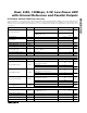
PARAMETER SYMBOL CONDITIONS MIN T YP MAX UNITS
Wake up from sleep mode 1
Wake-Up Time t
WAKE
Wake up from shutdown mode (Note 11) 20
µs
CHANNEL-TO-CHANNEL MATCHING
Crosstalk f
INA or B
= 20MHz at -1dB FS (Note 8) - 72 dB
Gain Matching f
INA or B
= 20MHz at -1dB FS (Note 9) 0.05 dB
Phase Matching f
INA or B
= 20MHz at -1dB FS (Note 10) ± 0.1 Degrees
ELECTRICAL CHARACTERISTICS (continued)
(V
DD
= 3.3V, OV
DD
= 2.5V, 0.1µF and 2.2µF capacitors from REFP, REFN, and COM to GND; REFOUT connected to REFIN through a
10kΩ resistor, V
IN
= 2V
P-P
(differential with respect to COM), C
L
= 10pF at digital outputs, f
CLK
= 100MHz, T
A
= T
MIN
to T
MAX
, unless
otherwise noted. ≥+25°C guaranteed by production test, <+25°C guaranteed by design and characterization. Typical values are at
T
A
= +25°C.)