
Instruction Manual

General Description
The MAX1209 is a 3.3V, 12-bit, 80Msps analog-to-digital
converter (ADC) featuring a fully differential wideband
track-and-hold (T/H) input amplifier, driving a low-noise
internal quantizer. The analog input stage accepts sin-
gle-ended or differential signals. The MAX1209 is opti-
mized for low power, small size, and high dynamic
performance. Excellent dynamic performance is main-
tained from baseband to input frequencies of 175MHz
and beyond, making the MAX1209 ideal for intermediate-
frequency (IF) sampling applications.
Powered from a single 3.0V to 3.6V supply, the
MAX1209 consumes only 366mW while delivering a
typical signal-to-noise (SNR) performance of 66.5dB at
an input frequency of 175MHz. In addition to low oper-
ating power, the MAX1209 features a 3µW power-down
mode to conserve power during idle periods.
A flexible reference structure allows the MAX1209 to use
the internal 2.048V bandgap reference or accept an
externally applied reference. The reference structure
allows the full-scale analog input range to be adjusted
from ±0.35V to ±1.15V. The MAX1209 provides a com-
mon-mode reference to simplify design and reduce exter-
nal component count in differential analog input circuits.
The MAX1209 supports both a single-ended and differ-
ential input clock drive. Wide variations in the clock
duty cycle are compensated with the ADC’s internal
duty-cycle equalizer (DCE).
ADC conversion results are available through a 12-bit,
parallel, CMOS-compatible output bus. The digital out-
put format is pin selectable to be either two’s comple-
ment or Gray code. A data-valid indicator eliminates
external components that are normally required for reli-
able digital interfacing. A separate digital power input
accepts a wide 1.7V to 3.6V supply, allowing the
MAX1209 to interface with various logic levels.
The MAX1209 is available in a 6mm x 6mm x 0.8mm,
40-pin thin QFN package with exposed paddle (EP),
and is specified for the extended industrial (-40°C to
+85°C) temperature range.
See the Pin-Compatible Versions table for a complete
family of 14-bit and 12-bit high-speed ADCs.
Applications
IF Communication Receivers
Cellular, Point-to-Point Microwave, HFC, WLAN
Ultrasound and Medical Imaging
Portable Instrumentation
Low-Power Data Acquisition
Features
♦ Direct IF Sampling Up to 400MHz
♦ Excellent Dynamic Performance
68.0dB/66.5dB SNR at f
IN
= 70MHz/175MHz
85.1dBc/85.5dBc SFDR at f
IN
= 70MHz/175MHz
♦ 3.3V Low-Power Operation
366mW (Single-Ended Clock Mode)
393mW (Differential Clock Mode)
3µW (Power-Down Mode)
♦ Differential or Single-Ended Clock
♦ Fully Differential or Single-Ended Analog Input
♦ Adjustable Full-Scale Analog Input Range: ±0.35V
to ±1.15V
♦ Common-Mode Reference
♦ CMOS-Compatible Outputs in Two’s Complement
or Gray Code
♦ Data-Valid Indicator Simplifies Digital Design
♦ Data Out-of-Range Indicator
♦ Miniature, 40-Pin Thin QFN Package with Exposed
Paddle
♦ Evaluation Kit Available (Order MAX1211EVKIT)
MAX1209
12-Bit, 80Msps, 3.3V IF-Sampling ADC
________________________________________________________________ Maxim Integrated Products 1
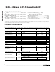
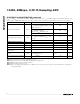
Ordering Information
19-1001; Rev 0; 8/04
For pricing, delivery, and ordering information, please contact Maxim/Dallas Direct! at
1-888-629-4642, or visit Maxim’s website at www.maxim-ic.com.
EVALUATION KIT
AVAILABLE
PART
TEMP
RANGE
PIN-PACKAGE
PKG
CODE
MAX1209ETL
-40°C to
+85°C
40 Thin QFN
(6mm x 6mm x 0.8mm)
T4066-3
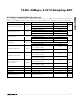
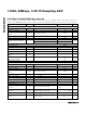
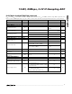
Pin-Compatible Versions
PART
SAMPLING
RATE (Msps)
RESOLUTION
(BITS)
TARGET
APPLICATION
MAX12553 65 14 IF/Baseband
MAX1209 80 12 IF
MAX1211 65 12 IF
MAX1208 80 12 Baseband
MAX1207 65 12 Baseband
MAX1206 40 12 Baseband
Pin Configuration appears at end of data sheet.