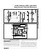
9-2851; Rev 1; 7/03 KIT ATION EVALU E L B A AVAIL 12-Bit 300ksps ADCs with FIFO, Temp Sensor, Internal Reference The MAX1231 is available in 28-pin 5mm x 5mm QFN with exposed pad and 24-pin QSOP packages. The MAX1227/MAX1229 are only available in QSOP packages. All three devices are specified over the extended -40°C to +85°C temperature range.
MAX1227/MAX1229/MAX1231 12-Bit 300ksps ADCs with FIFO, Temp Sensor, Internal Reference ABSOLUTE MAXIMUM RATINGS VDD to GND ..............................................................-0.3V to +6V CS, SCLK, DIN, EOC, DOUT to GND.........-0.3V to (VDD + 0.3V) AIN0–AIN13, REF-/AIN_, CNVST/AIN_, REF+ to GND.........................................-0.3V to (VDD + 0.3V) Maximum Current into Any Pin............................................50mA Continuous Power Dissipation (TA = +70°C) 16-Pin QSOP (derate 8.
12-Bit 300ksps ADCs with FIFO, Temp Sensor, Internal Reference (VDD = +2.7V to +3.6V, fSAMPLE = 300kHz, fSCLK = 4.8MHz (50% duty cycle), VREF = 2.5V, TA = TMIN to TMAX, unless otherwise noted. Typical values are at TA = +25°C.) PARAMETER SYMBOL CONDITIONS MIN TYP MAX UNITS CONVERSION RATE Power-Up Time tPU Acquisition Time tACQ Conversion Time tCONV External Clock Frequency fSCLK External reference 0.8 Internal reference (Note 3) 65 Internally clocked 3.5 µs 0.
MAX1227/MAX1229/MAX1231 12-Bit 300ksps ADCs with FIFO, Temp Sensor, Internal Reference ELECTRICAL CHARACTERISTICS (continued) (VDD = +2.7V to +3.6V, fSAMPLE = 300kHz, fSCLK = 4.8MHz (50% duty cycle), VREF = 2.5V, TA = TMIN to TMAX, unless otherwise noted. Typical values are at TA = +25°C.) PARAMETER SYMBOL CONDITIONS MIN TYP MAX UNITS DIGITAL INPUTS (SCLK, DIN, CS, CNVST) Input Voltage Low Input Voltage High Input Hysteresis VIL VDD x 0.3 VIH VDD x 0.
12-Bit 300ksps ADCs with FIFO, Temp Sensor, Internal Reference PARAMETER SYMBOL SCLK Clock Period tCP CONDITIONS MIN Externally clocked conversion 208 Data I/O 100 TYP MAX UNITS ns SCLK Duty Cycle tCH 60 % SCLK Fall to DOUT Transition tDOT CLOAD = 30pF 40 ns CS Rise to DOUT Disable tDOD CLOAD = 30pF 40 ns CS Fall to DOUT Enable tDOE CLOAD = 30pF DIN to SCLK Rise Setup tDS SCLK Rise to DIN Hold tDH CS to SCLK Rise Setup tCSS SCLK Rise to CS Hold tCSH 40 ns 40 tTS CS o
Typical Operating Characteristics (continued) (VDD = +3V, VREF = +2.5V, fSCLK = 4.8MHz, CLOAD = 30pF, TA = +25°C, unless otherwise noted.) SUPPLY CURRENT vs. SAMPLING RATE 60 40 MAX1227/29/31 toc05 500 400 0 200 10 100 1000 500 1 FREQUENCY (kHz) 10 100 1000 SUPPLY CURRENT vs. TEMPERATURE 625 MAX1227/29/31 toc07 0.4 fS = 300ksps SUPPLY CURRENT (µA) SHUTDOWN SUPPLY CURRENT (µA) 0.5 3.3 SUPPLY VOLTAGE (V) SHUTDOWN SUPPLY CURRENT vs. SUPPLY VOLTAGE 0.3 0.2 620 615 610 0.1 0 605 2.
12-Bit 300ksps ADCs with FIFO, Temp Sensor, Internal Reference 2.502 2.498 2.494 0.3 OFFSET ERROR (LSB) 0.2 OFFSET ERROR (LSB) 2.506 0.4 MAX1227/29/31 toc12 0.3 MAX1227/29/31 toc11 2.510 0.1 0 -0.1 -0.2 2.490 -15 10 35 60 TEMPERATURE (°C) 3.0 3.3 -0.1 -40 3.6 -15 35 60 85 GAIN ERROR vs. TEMPERATURE 1.5 GAIN ERROR (LSB) 1.0 MAX1227/29/31 toc15 2.0 MAX1227/29/31 toc14 1.5 10 TEMPERATURE (°C) GAIN ERROR vs. SUPPLY VOLTAGE 1.0 0.5 0.5 0 2.7 3.
12-Bit 300ksps ADCs with FIFO, Temp Sensor, Internal Reference MAX1227/MAX1229/MAX1231 Pin Description 8 MAX1231 QFN MAX1231 QSOP MAX1229 MAX1227 NAME 2–12, 26, 27, 28, 1–14 — — AIN0–13 — — 1–10 — AIN0–9 Analog Inputs — — — 1–6 AIN0–5 Analog Inputs 13 15 — — REF-/AIN14 Negative Input for External Differential Reference/Analog Input 14. See Table 3 for details on programming the setup register.
12-Bit 300ksps ADCs with FIFO, Temp Sensor, Internal Reference MAX1227/MAX1229/MAX1231 CS tCP tCH tCSS tCSH tCSH tCSS SCLK tDH tDS DIN tDOT tDOD tDOE DOUT Figure 1. Detailed Serial-Interface Timing Diagram CS DIN SCLK SERIAL INTERFACE OSCILLATOR CONTROL DOUT EOC CNVST AIN1 AIN2 T/H AIN15 12-BIT SAR ADC FIFO AND ACCUMULATOR TEMP SENSE REFREF+ INTERNAL REFERENCE MAX1227 MAX1229 MAX1231 Figure 2.
MAX1227/MAX1229/MAX1231 12-Bit 300ksps ADCs with FIFO, Temp Sensor, Internal Reference Converter Operation The MAX1227/MAX1229/MAX1231 ADCs use a fully differential, successive-approximation register (SAR) conversion technique and an on-chip T/H block to convert temperature and voltage signals into a 12-bit digital result. Both single-ended and differential configurations are supported, with a unipolar signal range for singleended mode and bipolar or unipolar ranges for differential mode.
12-Bit 300ksps ADCs with FIFO, Temp Sensor, Internal Reference CIN+ DAC COMPARATOR + HOLD GND (SINGLE ENDED); AIN1, AIN3, AIN5…AIN15 (DIFFERENTIAL) CIN- HOLD HOLD VDD/2 Figure 3. Equivalent Input Circuit Unipolar/Bipolar Address the unipolar and bipolar registers through the setup register (bits 1 and 0). Program a pair of analog channels for differential operation by writing a 1 to the appropriate bit of the bipolar or unipolar register.
MAX1227/MAX1229/MAX1231 12-Bit 300ksps ADCs with FIFO, Temp Sensor, Internal Reference Applications Information Register Descriptions The MAX1227/MAX1229/MAX1231 communicate between the internal registers and the external circuitry through the SPI/QSPI-compatible serial interface. Table 1 details the registers and the bit names. Tables 2–7 show the various functions within the conversion register, setup register, averaging register, reset register, unipolar register, and bipolar register.
12-Bit 300ksps ADCs with FIFO, Temp Sensor, Internal Reference BIT NAME — BIT FUNCTION 7 (MSB) Set to 1 to select conversion register. CHSEL3 6 Analog input channel select. CHSEL2 5 Analog input channel select. CHSEL1 4 Analog input channel select. CHSEL0 3 Analog input channel select. SCAN1 2 Scan mode select. SCAN0 1 Scan mode select. TEMP Set to 1 to take a single temperature 0 (LSB) measurement. The first conversion result of a scan contains temperature information.
MAX1227/MAX1229/MAX1231 12-Bit 300ksps ADCs with FIFO, Temp Sensor, Internal Reference Table 3. Setup Register* BIT NAME BIT FUNCTION — 7 (MSB) — 6 Set to 1 to select setup register. CKSEL1 5 Clock mode and CNVST configuration. Resets to 1 at power-up. CKSEL0 4 Clock mode and CNVST configuration. REFSEL1 3 Reference mode configuration. REFSEL0 2 Reference mode configuration. DIFFSEL1 1 Unipolar/bipolar mode register configuration for differential mode.
12-Bit 300ksps ADCs with FIFO, Temp Sensor, Internal Reference Output Data Format Figures 4–7 illustrate the conversion timing for the MAX1227/MAX1229/MAX1231. The 12-bit conversion result is output in MSB-first format with four leading zeros. DIN data is latched into the serial interface on the rising edge of SCLK. Data on DOUT transitions on the falling edge of SCLK. Conversions in clock modes 00 and 01 are initiated by CNVST.
MAX1227/MAX1229/MAX1231 12-Bit 300ksps ADCs with FIFO, Temp Sensor, Internal Reference Table 6. Averaging Register* BIT NAME BIT — 7 (MSB) Set to zero to select averaging register. FUNCTION — 6 Set to zero to select averaging register. Set to 1 to select averaging register. — 5 AVGON 4 Set to 1 to turn averaging on. Set to zero to turn averaging off. NAVG1 3 Configures the number of conversions for single-channel scans.
12-Bit 300ksps ADCs with FIFO, Temp Sensor, Internal Reference the internal oscillator. See Figure 5 for clock mode 01 timing. Performing Conversions in Clock Mode 00 In clock mode 00, the wake-up, acquisition, conversion, and shutdown sequences are initiated through CNVST and performed automatically using the internal oscillator. Results are added to the internal FIFO to be read out later. See Figure 4 for clock mode 00 timing.
MAX1227/MAX1229/MAX1231 12-Bit 300ksps ADCs with FIFO, Temp Sensor, Internal Reference CNVST (CONVERSION2) (ACQUISITION1) (ACQUISITION2) CS (CONVERSION1) SCLK DOUT LSB1 MSB1 MSB2 EOC REQUEST MULTIPLE CONVERSIONS BY SETTING CNVST LOW FOR EACH CONVERSION. Figure 5. Clock Mode 01 (CONVERSION BYTE) DIN (UP TO 514 INTERNALLY CLOCKED ACQUISITIONS AND CONVERSIONS) CS SCLK DOUT MSB1 LSB1 MSB2 EOC THE CONVERSION BYTE BEGINS THE ACQUISITION. CNVST IS NOT REQUIRED. Figure 6.
12-Bit 300ksps ADCs with FIFO, Temp Sensor, Internal Reference (ACQUISITION1) (CONVERSION1) (ACQUISITION2) CS SCLK DOUT MSB1 LSB1 MSB2 EOC EXTERNALLY TIMED ACQUISITION, SAMPLING AND CONVERSION WITHOUT CNVST. Figure 7.
MAX1227/MAX1229/MAX1231 12-Bit 300ksps ADCs with FIFO, Temp Sensor, Internal Reference OUTPUT CODE OUTPUT CODE FULL-SCALE TRANSITION 11 . . . 111 11 . . . 110 011 . . . 111 FS = VREF + VCOM 2 011 . . . 110 ZS = COM 11 . . . 101 000 . . . 010 000 . . . 001 FS = VREF + VCOM ZS = VCOM V 1 LSB = REF 4096 00 . . . 011 00 . . . 010 -VREF + VCOM 2 VREF 1 LSB = 4096 -FS = 000 . . . 000 111 . . . 111 111 . . . 110 111 . . . 101 100 . . . 001 00 . . . 001 100 . . . 000 00 . . .
12-Bit 300ksps ADCs with FIFO, Temp Sensor, Internal Reference THD = 20 x log (V 2 2 ) + V32 + V42 + V52 / V1 where V1 is the fundamental amplitude, and V2–V5 are the amplitudes of the first five harmonics. Spurious-Free Dynamic Range Spurious-free dynamic range (SFDR) is the ratio of the RMS amplitude of the fundamental (maximum signal component) to the RMS value of the next-largest distortion component.
Package Information (The package drawing(s) in this data sheet may not reflect the most current specifications. For the latest package outline information go to www.maxim-ic.com/packages.) QSOP.EPS MAX1227/MAX1229/MAX1231 12-Bit 300ksps ADCs with FIFO, Temp Sensor, Internal Reference PACKAGE OUTLINE, QSOP .150", .
12-Bit 300ksps ADCs with FIFO, Temp Sensor, Internal Reference 32L QFN.EPS PACKAGE OUTLINE, 16,20,28,32L QFN, 5x5x0.90 MM 1 21-0091 I 2 ______________________________________________________________________________________ 23 MAX1227/MAX1229/MAX1231 Package Information (continued) (The package drawing(s) in this data sheet may not reflect the most current specifications. For the latest package outline information go to www.maxim-ic.com/packages.
MAX1227/MAX1229/MAX1231 12-Bit 300ksps ADCs with FIFO, Temp Sensor, Internal Reference Package Information (continued) (The package drawing(s) in this data sheet may not reflect the most current specifications. For the latest package outline information go to www.maxim-ic.com/packages.) PACKAGE OUTLINE, 16,20,28,32L QFN, 5x5x0.90 MM 2 21-0091 I 2 Maxim cannot assume responsibility for use of any circuitry other than circuitry entirely embodied in a Maxim product.