
User Manual


MAX125/MAX126
2x4-Channel, Simultaneous-Sampling
14-Bit DAS
_______________________________________________________________________________________ 5
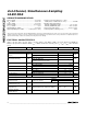
CONDITIONS
ns30t
CW
CONVST Pulse Width
UNITSMIN TYP MAXSYMBOLPARAMETER
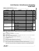
TIMING CHARACTERISTICS (Figure 4)
(AV
DD
= +5V, AV
SS
= -5V, DV
DD
= +5V, AGND = DGND = 0V, T
A
= T
MIN
to T
MAX
, unless otherwise noted.)
ns0t
CWS
CS to WR Setup Time
ns0t
CWH
CS to WR Hold Time
ns30t
WR
WR Low Pulse Width
ns125t
CSD
CS to CONVST Delay
ns30t
AS
Address Setup Time
ns0t
AH
Address Hold Time
25pF load ns30t
ID
RD to INT Delay
ns40t
RD
Delay Time Between Reads
ns0t
CRS
CS to RD Setup Time
ns0t
CRH
CS to RD Hold Time
ns30t
RD
RD Low Pulse Width
25pF load (Note 13) ns30t
DA
Data-Access Time
25pF load (Note 14) ns5 45t
DH
Bus-Relinquish Time
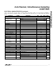
Mode 1, 1 channel
µs
3
Mode 2, 2 channel 6
Mode 3, 3 channel 9
Mode 4, 4 channel 12
t
CONV
Exiting shutdown µs5Start-Up Time
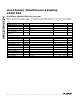
Note 1: AV
DD
= +5V, AV
SS
= -5V, DV
DD
= +5V, V
REFIN
= 2.500V (external), V
IN
= ±5V (MAX125) or ±2.5V (MAX126).
Note 2: Relative accuracy is the analog value’s deviation at any code from its theoretical value after the full-scale range has been
calibrated.
Note 3: CLK synchronized with CONVST.
Note 4: f
IN
= 10.06kHz, V
IN
= ±5V (MAX125) or ±2.5V (MAX126).
Note 5: First five harmonics.
Note 6: All inputs except CH1A driven with ±5V (MAX125) or ±2.5V (MAX126) 10kHz signal; CH1A connected to AGND and digitized.
Note 7: Guaranteed by design. Not production tested.
Note 8: AV
DD
= +5V, AV
SS
= -5V, DV
DD
= +5V, V
IN
= 0V (all channels).
Note 9: Temperature drift is defined as the change in output voltage from +25°C to T
MIN
or T
MAX
. It is calculated as
TC = [∆REFOUT/REFOUT] / ∆T.
Note 10: See Figure 2.
Note 11: Defined as the change in positive full scale caused by a ±5% variation in the nominal supply voltage. Tested with one input
at full scale and all others at AGND. V
REFIN
= 2.5V (internal).
Note 12: Tested with V
IN
= AGND on all channels, V
REFIN
= 2.5V (internal).
Note 13: The data-access time is defined as the time required for an output to cross 0.8V or 2.0V. It is measured using the circuit of
Figure 1. The measured number is then extrapolated back to determine the value with a 25pF load.
Note 14: The bus-relinquish time is derived from the measured time taken for the data outputs to change 0.5V when loaded with the
circuit of Figure 1. The measured number is then extrapolated back to remove the effects of charging/discharging the 120pF
capacitor. Thus, the time given is the part’s true bus-relinquish time, independent of the external bus loading capacitance.
Conversion Time
Mode 1, 1 channel
ksps
250
Conversion Rate/Channel
Mode 2, 2 channel 142
Mode 3, 3 channel 100
Mode 4, 4 channel 76