
User Manual


_______________Detailed Description
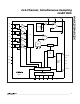
The MAX125/MAX126 use a successive-approximation
conversion technique and four simultaneous-sampling
track/hold (T/H) amplifiers to convert analog signals into
14-bit digital outputs. Each T/H has two multiplexed
inputs, allowing a total of eight inputs. Each T/H output
is converted and stored in memory to be accessed
sequentially by the parallel interface with successive
read cycles. The MAX125/MAX126 internal micro-
sequencer can be programmed to digitize one, two,
three, or four inputs sampled simultaneously from either
of the two banks of four inputs (see Figure 2).
The conversion timing and control sequences are
derived from a 16MHz external clock, the CONVST
MAX125/MAX126
2x4-Channel, Simultaneous-Sampling
14-Bit DAS
6 _______________________________________________________________________________________
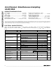
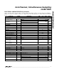
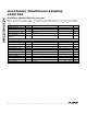
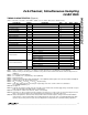
NAME FUNCTION
1, 2 CH2B, CH2A Channel 2 Multiplexed Inputs, single-ended
3, 4 CH1B, CH1A Channel 1 Multiplexed Inputs, single-ended
PIN
5 AV
DD
+5V ±5% Analog Supply Voltage
6 REFIN External Reference Input/Internal Reference Output. Bypass with a 0.1µF capacitor to AGND.
17 DV
DD
+5V ±5% Digital Supply Voltage
9–16 D13–D6 Data Bits. D13 = MSB.
8, 36 AGND Analog Ground. Both pins must be tied to ground.
7 REFOUT Reference-Buffer Output. Bypass with a 4.7µF capacitor to AGND.
26
CS
Chip-Select Input (active-low)
25 CLK Clock Input (duty cycle must be 30% to 70%).
21–24 D3/A3–D0/A0 Bidirectional Data Bits/Address Bits. D0/A0 = LSB.
19, 20 D5, D4 Data Bits
18 DGND Digital Ground
______________________________________________________________Pin Description
27
WR
Write Input (active-low)
28
RD
Read Input (active-low)
29
CONVST
Conversion-Start Input. Rising edge initiates sampling and conversion sequence.
30
INT
Interrupt Output. Falling edge indicates the end of a conversion sequence.
31 AV
SS
-5V ±5% Analog Supply Voltage
32, 33 CH4A, CH4B Channel 4 Multiplexed Inputs, single-ended
34, 35 CH3A, CH3B Channel 3 Multiplexed Inputs, single-ended
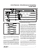
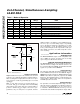
Figure 1. Load Circuit for Access Time and Bus Relinquish Time
TO OUTPUT
PIN
120pF
1.0mA
1.6mA
1.6V