
User Manual


MAX125/MAX126
2x4-Channel, Simultaneous-Sampling
14-Bit DAS
8 _______________________________________________________________________________________
signal, and the programmed mode. The T/H amplifiers
hold the input voltages at the CONVST rising edge.
Additional CONVST pulses are ignored until the last
conversion for the sample is complete. The ADC con-
verts each assigned channel in 3µs and stores the
result in an internal 4x14-bit memory.
At the end of the last conversion, INT goes low and the
T/H amplifiers begin to track the inputs again. The data
can be accessed by applying successive pulses to the
RD pin. Successive reads access data words sequen-
tially. The memory is
not
random-access; data from
CH1 is always read first. After accessing all pro-
grammed channels, the address pointer selects CH1
again. Additional read pulses cycle through the data
words. CS can be held low during successive reads.
Input Bandwidth
The T/H’s input tracking circuitry has an 8MHz small-
signal bandwidth, so it is possible to digitize high-
speed transient events and measure periodic signals
with bandwidths exceeding the ADC’s sampling rate by
using undersampling techniques. To avoid high-
frequency signals being aliased into the frequency
band of interest, anti-alias filtering is recommended.
Analog Input Range and Input Protection
The MAX125’s input range is ±5V, and the MAX126’s
input range is ±2.5V. The input resistance for both parts
is 10kΩ. An input protection structure allows input volt-
ages to ±17V without harming the IC. This protection is
also active in shutdown mode.
Track/Holds
The MAX125/MAX126 feature four simultaneous T/Hs.
Each T/H has two multiplexed inputs. A T-switch input
configuration provides excellent hold-mode isolation.
Allow 1µs acquisition time for 14-bit accuracy.
The T/H aperture delay is typically 10ns. The 500ps
aperture-delay mismatch between the T/Hs allows the
relative phase information of up to four different inputs
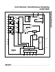
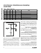
to be preserved. Figure 3 shows the equivalent input
circuit, illustrating the ADC’s sampling architecture.
Only one of four T/H stages with its two multiplexed
inputs (CH_A and CH_B) is shown. All switches are in
track configuration for channel A. An internal buffer
charges the hold capacitor to minimize the required
acquisition time between conversions. The analog input
appears as a 10kΩ resistor in parallel with a 16pF
capacitor.
C
IN
5k
C
IN
5k
S1A S2A
HOLD
BUFFER
TRACK
C
HOLD
7pF
HOLD
FROM MICROSEQUENCER
REFOUT
TRACK
MUX
DAC
SAR
S1B S2B
S3B
S3A
5k
5k
CH_A
CH_B
MAX125
MAX126
Figure 3. Equivalent Input Circuit