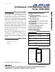
9-3575; Rev 1; 11/06 8-/4-Channel, ±12V Multirange Inputs, Serial 16-Bit ADCs The MAX1300/MAX1301 multirange, low-power, 16-bit, successive-approximation, analog-to-digital converters (ADCs) operate from a single +5V supply and achieve throughput rates up to 115ksps. A separate digital supply allows digital interfacing with 2.7V to 5.25V systems using the SPI™-/QSPI™-/MICROWIRE™-compatible serial interface. Partial power-down mode reduces the supply current to 1.3mA (typ).
MAX1300/MAX1301 8-/4-Channel, ±12V Multirange Inputs, Serial 16-Bit ADCs ABSOLUTE MAXIMUM RATINGS AVDD1 to AGND1 ....................................................-0.3V to +6V AVDD2 to AGND2 ....................................................-0.3V to +6V DVDD to DGND ........................................................-0.3V to +6V DVDDO to DGNDO ..................................................-0.3V to +6V DVDD to DVDDO ......................................................-0.
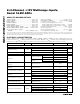
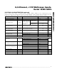
8-/4-Channel, ±12V Multirange Inputs, Serial 16-Bit ADCs (AVDD1 = AVDD2 = DVDD = DVDDO = 5V, AGND1 = DGND = DGNDO = AGND2 = AGND3 = 0, fCLK = 3.5MHz (50% duty cycle), external clock mode, VREF = 4.096V (external reference operation), REFCAP = AVDD1, maximum single-ended bipolar input range (±12V), CDOUT = 50pF, CSSTRB = 50pF, TA = -40°C to +85°C, unless otherwise noted. Typical values are at TA = +25°C.
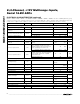
MAX1300/MAX1301 8-/4-Channel, ±12V Multirange Inputs, Serial 16-Bit ADCs ELECTRICAL CHARACTERISTICS (continued) (AVDD1 = AVDD2 = DVDD = DVDDO = 5V, AGND1 = DGND = DGNDO = AGND2 = AGND3 = 0, fCLK = 3.5MHz (50% duty cycle), external clock mode, VREF = 4.096V (external reference operation), REFCAP = AVDD1, maximum single-ended bipolar input range (±12V), CDOUT = 50pF, CSSTRB = 50pF, TA = -40°C to +85°C, unless otherwise noted. Typical values are at TA = +25°C.
8-/4-Channel, ±12V Multirange Inputs, Serial 16-Bit ADCs (AVDD1 = AVDD2 = DVDD = DVDDO = 5V, AGND1 = DGND = DGNDO = AGND2 = AGND3 = 0, fCLK = 3.5MHz (50% duty cycle), external clock mode, VREF = 4.096V (external reference operation), REFCAP = AVDD1, maximum single-ended bipolar input range (±12V), CDOUT = 50pF, CSSTRB = 50pF, TA = -40°C to +85°C, unless otherwise noted. Typical values are at TA = +25°C.) PARAMETER SYMBOL CONDITIONS MIN TYP MAX UNITS Preamplifier Supply Voltage AVDD2 4.75 5.
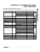
ELECTRICAL CHARACTERISTICS (continued) (AVDD1 = AVDD2 = DVDD = DVDDO = 5V, AGND1 = DGND = DGNDO = AGND2 = AGND3 = 0, fCLK = 3.5MHz (50% duty cycle), external clock mode, VREF = 4.096V (external reference operation), REFCAP = AVDD1, maximum single-ended bipolar input range (±12V), CDOUT = 50pF, CSSTRB = 50pF, TA = -40°C to +85°C, unless otherwise noted. Typical values are at TA = +25°C.
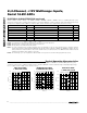
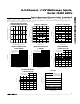
8-/4-Channel, ±12V Multirange Inputs, Serial 16-Bit ADCs DIGITAL I/O SUPPLY CURRENT vs. DIGITAL I/O SUPPLY VOLTAGE ANALOG SUPPLY CURRENT vs. ANALOG SUPPLY VOLTAGE 0.24 MAX1300/01 toc05 EXTERNAL CLOCK MODE 0.26 PARTIAL POWER-DOWN MODE 0.53 +85°C 0.22 +85°C 0.20 IAVDD1 (mA) IDVDDO (mA) 0.55 MAX1300/01 toc04 0.28 +25°C 0.18 0.16 0.51 +25°C 0.49 -40°C -40°C 0.14 0.47 0.12 0.10 0.45 4.75 4.85 4.95 5.05 5.15 4.75 4.85 4.95 5.05 5.
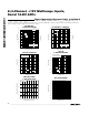
Typical Operating Characteristics (continued) (AVDD1 = AVDD2 = DVDD = DVDDO = 5V, AGND1 = DGND = DGNDO = AGND2 = AGND3 = 0, fCLK = 3.5MHz (50% duty cycle), external clock mode, VREF = 4.096V (external reference operation), REFCAP = AVDD1, maximum single-ended bipolar input range, CDOUT = 50pF, CSSTRB = 50pF; unless otherwise noted.) PREAMPLIFIER SUPPLY CURRENT vs. CONVERSION RATE ANALOG SUPPLY CURRENT vs. CONVERSION RATE MAX1300/01 toc09 EXTERNAL CLOCK MODE 2.5 25 MAX1300/01 toc08 3.0 fCLK = 7.
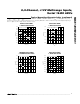
8-/4-Channel, ±12V Multirange Inputs, Serial 16-Bit ADCs EXTERNAL REFERENCE INPUT CURRENT vs. EXTERNAL REFERENCE INPUT VOLTAGE 0.13 0.04 ±12V BIPOLAR RANGE 0.02 0 -0.02 -0.04 0.8 0.6 ±3V BIPOLAR RANGE -0.06 3.85 3.90 3.95 4.00 4.05 ±12V BIPOLAR RANGE -1.0 -15 -40 10 35 60 -40 85 -15 10 35 CHANNEL-TO-CHANNEL ISOLATION vs. INPUT FREQUENCY COMMON-MODE REJECTION RATIO vs. FREQUENCY INTEGRAL NONLINEARITY vs. DIGITAL OUTPUT CODE fSAMPLE = 115ksps ±12V BIPOLAR RANGE -20 1.
Typical Operating Characteristics (continued) (AVDD1 = AVDD2 = DVDD = DVDDO = 5V, AGND1 = DGND = DGNDO = AGND2 = AGND3 = 0, fCLK = 3.5MHz (50% duty cycle), external clock mode, VREF = 4.096V (external reference operation), REFCAP = AVDD1, maximum single-ended bipolar input range, CDOUT = 50pF, CSSTRB = 50pF; unless otherwise noted.) SNR, SINAD, ENOB vs. ANALOG INPUT FREQUENCY SNR, SINAD, ENOB vs.
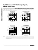
8-/4-Channel, ±12V Multirange Inputs, Serial 16-Bit ADCs FULL-POWER BANDWIDTH REFERENCE VOLTAGE vs.
MAX1300/MAX1301 8-/4-Channel, ±12V Multirange Inputs, Serial 16-Bit ADCs Pin Description PIN MAX1300 MAX1301 12 NAME FUNCTION Analog Supply Voltage 1. Connect AVDD1 to a +4.75V to +5.25V power-supply voltage. Bypass AVDD1 to AGND1 with a 0.1µF capacitor.
8-/4-Channel, ±12V Multirange Inputs, Serial 16-Bit ADCs PIN MAX1300 MAX1301 NAME FUNCTION 21 18 AGND3 Analog Signal Ground 3. AGND3 is the ADC negative reference potential. Connect AGND3 to AGND1. DGND, DGNDO, AGND3, AGND2, and AGND1 must be connected together. 22 19 AVDD2 Analog Supply Voltage 2. Connect AVDD2 to a +4.75V to +5.25V power-supply voltage. Bypass AVDD2 to AGND2 with a 0.1µF capacitor. 23 20 AGND2 Analog Ground 2.
MAX1300/MAX1301 8-/4-Channel, ±12V Multirange Inputs, Serial 16-Bit ADCs Power Supplies Track-and-Hold Circuitry To maintain a low-noise environment, the MAX1300 and MAX1301 provide separate power supplies for each section of circuitry. Table 1 shows the four separate power supplies. Achieve optimal performance using separate AVDD1, AVDD2, DVDD, and DVDDO supplies. Alternatively, connect AV DD1 , AV DD2 , and DV DD together as close to the device as possible for a convenient power connection.
8-/4-Channel, ±12V Multirange Inputs, Serial 16-Bit ADCs MAX1300/MAX1301 CS 32 31 30 BYTE 3 29 28 27 26 25 24 23 22 BYTE 2 21 20 19 18 17 16 15 14 13 BYTE 1 12 11 9 10 8 7 6 5 4 3 2 1 SCLK BYTE 4 SSTRB DIN S C2 C1 C0 0 0 0 0 fSAMPLE ≈ fSCLK / 32 SAMPLING INSTANT tACQ ANALOG INPUT TRACK AND HOLD* DOUT HOLD TRACK HIGH IMPEDANCE HOLD B15 B14 B13 B12 B11 B10 B9 B8 B7 B6 B5 B4 B3 B2 B1 B0 HIGH IMPEDANCE *TRACK AND HOLD TIMING IS CONTROLLED B
MAX1300/MAX1301 8-/4-Channel, ±12V Multirange Inputs, Serial 16-Bit ADCs CS SSTRB 32 31 30 BYTE 3 29 28 27 26 25 24 23 0 22 BYTE 2 21 20 19 0 18 0 17 C0 16 C1 15 C2 14 S 13 DIN 12 BYTE 1 11 9 10 8 7 6 5 4 3 2 1 SCLK BYTE 4 0 HIGH IMPEDANCE DOUT B15 B14 B13 B12 B11 B10 B9 B8 B7 B6 B5 B4 B3 B2 B1 B0 fSAMPLE ≈ fSCLK / 32 + fINTCLK / 17 SAMPLING INSTANT tACQ ANALOG INPUT TRACK AND HOLD* HOLD TRACK HOLD 100ns to 400ns 17 16 15 14 3 2
8-/4-Channel, ±12V Multirange Inputs, Serial 16-Bit ADCs MAX1300/MAX1301 CS SSTRB 24 23 0 22 BYTE 2 21 0 20 0 19 C0 18 C1 17 C2 16 S 15 DIN 14 BYTE 1 13 12 11 9 10 8 7 6 5 4 3 2 1 SCLK BYTE 3 0 HIGH IMPEDANCE DOUT B15 B14 B13 B12 B11 B10 B9 B8 B7 B6 B5 B4 B3 B2 B1 B0 fSAMPLE ≈ fSCLK / 24 + fINTCLK / 28 SAMPLING INSTANT tACQ ANALOG INPUT TRACK AND HOLD* TRACK HOLD HOLD 100ns to 400ns 28 27 26 25 14 13 12 11 10 3 2 1 INTCLK** fINTCLK
MAX1300/MAX1301 8-/4-Channel, ±12V Multirange Inputs, Serial 16-Bit ADCs Table 3. Input Data Word Formats DATA BIT OPERATION D7 (START) D6 D5 D4 D3 D2 D1 D0 Conversion-Start Byte (Tables 4 and 5) 1 C2 C1 C0 0 0 0 0 Analog-Input Configuration Byte (Table 2) 1 C2 C1 C0 DIF/SGL R2 R1 R0 Mode-Control Byte (Table 7) 1 M2 M1 M0 1 0 0 0 CH6 CH7 Table 4.
8-/4-Channel, ±12V Multirange Inputs, Serial 16-Bit ADCs +9 +18 FSR = 12V +24 FSR = 12V INPUT RANGE SELECTION BITS, R[2:0] EACH INPUT IS FAULT TOLERANT TO ±16.5V. VREF = 4.096V. Figure 7. Single-Ended Input Voltage Ranges Digital Interface The MAX1300/MAX1301 feature a serial interface that is compatible with SPI/QSPI and MICROWIRE devices.
MAX1300/MAX1301 8-/4-Channel, ±12V Multirange Inputs, Serial 16-Bit ADCs Table 6.
12 8 8 COMMON-MODE VOLTAGE (V) 12 4 0 -4 -8 -12 4 0 -4 -8 -12 -16 -16 -18 -12 -6 0 6 12 18 -18 -12 INPUT VOLTAGE (V) Figure 9. Common-Mode Voltage vs. Input Voltage (FSR = 12V) 0 6 12 18 Figure 10. Common-Mode Voltage vs. Input Voltage (FSR = 24V) Output Data Format Output data is clocked out of DOUT in offset binary format on the falling edge of SCLK, MSB first (B15). For output binary codes, see the Transfer Function section and Figures 12, 13, and 14.
MAX1300/MAX1301 8-/4-Channel, ±12V Multirange Inputs, Serial 16-Bit ADCs FSR FSR FFFF FFFE FFFD 8001 8000 7FFF 8001 FSR BINARY OUTPUT CODE (LSB [hex]) FFFE FFFD FSR BINARY OUTPUT CODE (LSB [hex]) FFFF 8000 7FFF 0003 0003 0002 0002 1 LSB = FSR x VREF 65,536 x 4.096V 0001 1 LSB = 0001 FSR x VREF 65,536 x 4.096V 0000 0000 -32,768 -32,766 -1 0 +1 0 +32,765 +32,767 1 2 3 32,768 65,533 65,535 INPUT VOLTAGE (LSB [DECIMAL]) (AGND1) AGND1 (DIF/SGL = 0) OV (DIF/SGL = 1) Figure 13.
8-/4-Channel, ±12V Multirange Inputs, Serial 16-Bit ADCs CS tCL SCLK tCH tCSH 1 8 tCP tDS DIN START SEL2 SEL1 SEL0 1 8 tDH DIF/SGL R2 R1 R0 START M2 ANALOG INPUT CONFIGURATION BYTE tDV DOUT M1 M0 1 0 0 0 MODE CONTROL BYTE tTR HIGH IMPEDANCE HIGH IMPEDANCE HIGH IMPEDANCE Figure 15. Analog Input Configuration Byte and Mode-Control Byte Timing SSTRB tSSCS CS tCSS SCLK tDO DOUT HIGH IMPEDANCE MSB NOTE: SSTRB AND CS REMAIN LOW IN EXTERNAL CLOCK MODE (MODE 0).
MAX1300/MAX1301 8-/4-Channel, ±12V Multirange Inputs, Serial 16-Bit ADCs Table 8. Mode-Control Bits M[2:0] M2 M1 M0 0 0 0 External Clock (DEFAULT) MODE 0 0 1 External Acquisition 0 1 0 Internal Clock 0 1 1 Reserved 1 0 0 Reset 1 0 1 Reserved 1 1 0 Partial Power-Down 1 1 1 Full Power-Down External Acquisition Mode (Mode 1) The slowest maximum throughput rate is achieved with the external acquisition method.
8-/4-Channel, ±12V Multirange Inputs, Serial 16-Bit ADCs REF. When using the internal reference, bypass REFCAP with a 0.1µF or greater capacitor to AGND1 and bypass REF with a 1.0µF or greater capacitor to AGND1. • Partial Power-Down-Mode Control Byte This prevents the MAX1300/MAX1301 from inadvertently exiting full power-down mode because of a CS glitch in a noisy digital environment.
MAX1300/MAX1301 8-/4-Channel, ±12V Multirange Inputs, Serial 16-Bit ADCs V+ 1.0µF IN 4.096V SAR ADC REF REF OUT 1.0µF MAX6341 AVDD1 1x REFCAP MAX1300 MAX1301 GND 5kΩ VRCTH 4.096V BANDGAP REFERENCE AGND1 Figure 18. External Reference Operation Bridge Application Layout, Grounding, and Bypassing The MAX1300/MAX1301 convert 1kHz signals more accurately than a similar sigma-delta converter that might be considered in bridge applications.
8-/4-Channel, ±12V Multirange Inputs, Serial 16-Bit ADCs MAX1300/MAX1301 4–20mA INPUT CH0 µC 250Ω MAX1300 4–20mA INPUT CH8 250Ω Figure 19. 4–20mA Application LOW-OFFSET DIFFERENTIAL AMPLIFIER CH0 µP CH1 MAX1300 MAX1301 REF BRIDGE Figure 20. Bridge Application Differential Nonlinearity (DNL) Channel-to-Channel Isolation DNL is the difference between an actual step width and the ideal value of 1 LSB.
MAX1300/MAX1301 8-/4-Channel, ±12V Multirange Inputs, Serial 16-Bit ADCs Unipolar Offset Error -FSR to 0V When a zero-scale analog input voltage is applied to the converter inputs, the digital output is all ones (0xFFFF). Ideally, the transition from 0xFFFF to 0xFFFE occurs at AGND1 - 0.5 LSB. Unipolar offset error is the amount of deviation between the measured zero-scale transition point and the ideal zero-scale transition point, with all untested channels grounded.
8-/4-Channel, ±12V Multirange Inputs, Serial 16-Bit ADCs SINAD − 1.76 ENOB = 6.02 SCLK (MODE 0) 13 14 SCLK (MODE 1) 15 16 INTCLK (MODE 2) 10 11 MAX1300/MAX1301 Effective Number of Bits (ENOB) ENOB indicates the global accuracy of an ADC at a specific input frequency and sampling rate.
8-/4-Channel, ±12V Multirange Inputs, Serial 16-Bit ADCs MAX1300/MAX1301 Block Diagram SERIAL I/O CONTROL LOGIC AND REGISTERS AVDD2 CH0 CH1 CH2 CH3 CH4 CH5 CH6 CH7 AGND1 CLOCK ANALOG INPUT MUX AND MULTIRANGE CIRCUITRY PGA IN SAR ADC OUT DVDD FIFO DGND AVDD1 AGND3 REF AGND2 4.
8-/4-Channel, ±12V Multirange Inputs, Serial 16-Bit ADCs TSSOP4.40mm.EPS PACKAGE OUTLINE, TSSOP 4.40mm BODY 21-0066 G 1 1 Maxim cannot assume responsibility for use of any circuitry other than circuitry entirely embodied in a Maxim product. No circuit patent licenses are implied. Maxim reserves the right to change the circuitry and specifications without notice at any time.