9-3052; Rev 3; 8/04 8-/4-/2-Channel, 12-Bit, Simultaneous-Sampling ADCs with ±10V, ±5V, and 0 to +5V Analog Input Ranges The MAX1304–MAX1306/MAX1308–MAX1310/MAX1312– MAX1314 12-bit, analog-to-digital converters (ADCs) offer eight, four, or two independent input channels. Independent track-and-hold (T/H) circuitry provides simultaneous sampling for each channel. The MAX1304/ MAX1305/MAX1306 provide a 0 to +5V input range with ±6V fault-tolerant inputs.
MAX1304–MAX1306/MAX1308–MAX1310/MAX1312–MAX1314 8-/4-/2-Channel, 12-Bit, Simultaneous-Sampling ADCs with ±10V, ±5V, and 0 to +5V Analog Input Ranges ABSOLUTE MAXIMUM RATINGS AVDD to AGND .........................................................-0.3V to +6V DVDD to DGND.........................................................-0.3V to +6V AGND to DGND.....................................................-0.3V to +0.3V CH0–CH7, I.C. to AGND (MAX1304/MAX1305/MAX1306)....±6V CH0–CH7, I.C.
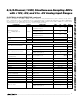
8-/4-/2-Channel, 12-Bit, Simultaneous-Sampling ADCs with ±10V, ±5V, and 0 to +5V Analog Input Ranges (AVDD = +5V, DVDD = +3V, AGND = DGND = 0, VREF = VREFMS = +2.5V (external reference), CREF = CREFMS = 0.1µF, CREF+ = CREF- = 0.1µF, CREF+-to-REF- = 2.2µF || 0.1µF, CCOM = 2.2µF || 0.1µF, CMSV = 2.2µF || 0.1µF (unipolar devices), MSV = AGND (bipolar devices), fCLK = 16.67MHz 50% duty cycle, INTCLK/EXTCLK = AGND (external clock), SHDN = DGND, TA = TMIN to TMAX, unless otherwise noted.
MAX1304–MAX1306/MAX1308–MAX1310/MAX1312–MAX1314 8-/4-/2-Channel, 12-Bit, Simultaneous-Sampling ADCs with ±10V, ±5V, and 0 to +5V Analog Input Ranges ELECTRICAL CHARACTERISTICS (continued) (AVDD = +5V, DVDD = +3V, AGND = DGND = 0, VREF = VREFMS = +2.5V (external reference), CREF = CREFMS = 0.1µF, CREF+ = CREF- = 0.1µF, CREF+-to-REF- = 2.2µF || 0.1µF, CCOM = 2.2µF || 0.1µF, CMSV = 2.2µF || 0.1µF (unipolar devices), MSV = AGND (bipolar devices), fCLK = 16.
8-/4-/2-Channel, 12-Bit, Simultaneous-Sampling ADCs with ±10V, ±5V, and 0 to +5V Analog Input Ranges (AVDD = +5V, DVDD = +3V, AGND = DGND = 0, VREF = VREFMS = +2.5V (external reference), CREF = CREFMS = 0.1µF, CREF+ = CREF- = 0.1µF, CREF+-to-REF- = 2.2µF || 0.1µF, CCOM = 2.2µF || 0.1µF, CMSV = 2.2µF || 0.1µF (unipolar devices), MSV = AGND (bipolar devices), fCLK = 16.67MHz 50% duty cycle, INTCLK/EXTCLK = AGND (external clock), fIN = 500kHz, AIN = -0.4dBFS. TA = +25°C, unless otherwise noted.
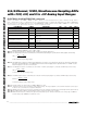
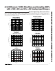
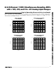
Typical Operating Characteristics (continued) (AVDD = +5V, DVDD = +3V, AGND = DGND = 0, VREF = VREFMS = +2.5V (external reference), CREF = CREFMS = 0.1µF, CREF+ = CREF- = 0.1µF, CREF+-to-REF- = 2.2µF || 0.1µF, CCOM = 2.2µF || 0.1µF, CMSV = 2.2µF || 0.1µF (unipolar devices), MSV = AGND (bipolar devices), fCLK = 16.67MHz 50% duty cycle, INTCLK/EXTCLK = AGND (external clock), fIN = 500kHz, AIN = -0.4dBFS. TA = +25°C, unless otherwise noted.) (Figures 3 and 4) SMALL-SIGNAL BANDWIDTH vs.
8-/4-/2-Channel, 12-Bit, Simultaneous-Sampling ADCs with ±10V, ±5V, and 0 to +5V Analog Input Ranges (AVDD = +5V, DVDD = +3V, AGND = DGND = 0, VREF = VREFMS = +2.5V (external reference), CREF = CREFMS = 0.1µF, CREF+ = CREF- = 0.1µF, CREF+-to-REF- = 2.2µF || 0.1µF, CCOM = 2.2µF || 0.1µF, CMSV = 2.2µF || 0.1µF (unipolar devices), MSV = AGND (bipolar devices), fCLK = 16.67MHz 50% duty cycle, INTCLK/EXTCLK = AGND (external clock), fIN = 500kHz, AIN = -0.4dBFS. TA = +25°C, unless otherwise noted.
Typical Operating Characteristics (continued) (AVDD = +5V, DVDD = +3V, AGND = DGND = 0, VREF = VREFMS = +2.5V (external reference), CREF = CREFMS = 0.1µF, CREF+ = CREF- = 0.1µF, CREF+-to-REF- = 2.2µF || 0.1µF, CCOM = 2.2µF || 0.1µF, CMSV = 2.2µF || 0.1µF (unipolar devices), MSV = AGND (bipolar devices), fCLK = 16.67MHz 50% duty cycle, INTCLK/EXTCLK = AGND (external clock), fIN = 500kHz, AIN = -0.4dBFS. TA = +25°C, unless otherwise noted.) (Figures 3 and 4) SIGNAL-TO-NOISE PLUS DISTORTION vs.
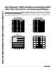
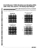
8-/4-/2-Channel, 12-Bit, Simultaneous-Sampling ADCs with ±10V, ±5V, and 0 to +5V Analog Input Ranges TA = +85°C 56 2.0 MAX1304 toc19 57 CLOAD = 50pF 1.8 TA = +85°C 1.6 IDVDD (mA) IAVDD (mA) 55 TA = +25°C 54 TA = +25°C 1.4 TA = -40°C 1.2 TA = -40°C 53 1.0 52 0.8 0.6 51 4.7 4.8 4.9 5.0 5.1 2.5 5.3 5.2 3.0 3.5 4.0 4.5 5.5 5.0 DVDD (V) AVDD (V) DIGITAL SHUTDOWN CURRENT vs. DIGITAL SUPPLY VOLTAGE ANALOG SHUTDOWN CURRENT vs.
Typical Operating Characteristics (continued) (AVDD = +5V, DVDD = +3V, AGND = DGND = 0, VREF = VREFMS = +2.5V (external reference), CREF = CREFMS = 0.1µF, CREF+ = CREF- = 0.1µF, CREF+-to-REF- = 2.2µF || 0.1µF, CCOM = 2.2µF || 0.1µF, CMSV = 2.2µF || 0.1µF (unipolar devices), MSV = AGND (bipolar devices), fCLK = 16.67MHz 50% duty cycle, INTCLK/EXTCLK = AGND (external clock), fIN = 500kHz, AIN = -0.4dBFS. TA = +25°C, unless otherwise noted.
8-/4-/2-Channel, 12-Bit, Simultaneous-Sampling ADCs with ±10V, ±5V, and 0 to +5V Analog Input Ranges PIN MAX1304 MAX1308 MAX1312 MAX1305 MAX1309 MAX1313 MAX1306 MAX1310 MAX1314 NAME FUNCTION 1, 15, 17 1, 15, 17 1, 15, 17 AVDD Analog Power Input. AVDD is the power input for the analog section of the converter. Apply +5V to AVDD. Connect all AVDD pins together. See the Layout, Grounding, and Bypassing section for additional information.
MAX1304–MAX1306/MAX1308–MAX1310/MAX1312–MAX1314 8-/4-/2-Channel, 12-Bit, Simultaneous-Sampling ADCs with ±10V, ±5V, and 0 to +5V Analog Input Ranges Pin Description (continued) PIN MAX1304 MAX1308 MAX1312 MAX1305 MAX1309 MAX1313 MAX1306 MAX1310 MAX1314 NAME FUNCTION 20 20 20 REF+ Positive Reference Bypass. Bypass REF+ with a 0.1µF capacitor to AGND. Also bypass REF+ to REF- with a 2.2µF and a 0.1µF capacitor. VREF+ = VCOM + VREF / 2. 21 21 21 COM Reference Common Bypass.
8-/4-/2-Channel, 12-Bit, Simultaneous-Sampling ADCs with ±10V, ±5V, and 0 to +5V Analog Input Ranges PIN MAX1304 MAX1308 MAX1312 MAX1305 MAX1309 MAX1313 MAX1306 MAX1310 MAX1314 NAME FUNCTION 44 44 44 CS Chip-Select Input. Pulling CS low activates the digital interface. Forcing CS high places D0–D11 in high-impedance mode. 45 45 45 CONVST 46 46 46 CLK 47 47 47 SHDN Conversion Start Input. Driving CONVST high initiates the conversion process.
MAX1304–MAX1306/MAX1308–MAX1310/MAX1312–MAX1314 8-/4-/2-Channel, 12-Bit, Simultaneous-Sampling ADCs with ±10V, ±5V, and 0 to +5V Analog Input Ranges MAX1304–MAX1306 MAX1308–MAX1310 MAX1312–MAX1314 AVDD CH0 DVDD D11 T/H 12-BIT ADC 8x1 MUX CH7 D8 8 x 12 SRAM OUTPUT DRIVERS T/H D7 D0 MSV CONFIGURATION REGISTER * WR CS REF+ COM REF- INTERFACE AND CONTROL RD CONVST SHDN 5kΩ INTCLK/EXTCLK REF CLK 5kΩ CHSHDN REFMS EOC 2.
8-/4-/2-Channel, 12-Bit, Simultaneous-Sampling ADCs with ±10V, ±5V, and 0 to +5V Analog Input Ranges DVDD 0.1µF 1 0.1µF 15 0.1µF 17 BIPOLAR CONFIGURATION 18 0.01µF 19 AVDD DGND AVDD CLK REFMS MAX1308 MAX1312 CONVST CS WR 0.1µF 20 REF+ 0.1µF 2.2µF RD EOLC 22 REF0.1µF SHDN MSV REF EOC 24, 39 GND 48 47 46 45 44 43 DIGITAL INTERFACE AND CONTROL 42 41 40 2.2µF D11 21 0.1µF GND +2.7V TO +5.25V 0.
MAX1304–MAX1306/MAX1308–MAX1310/MAX1312–MAX1314 8-/4-/2-Channel, 12-Bit, Simultaneous-Sampling ADCs with ±10V, ±5V, and 0 to +5V Analog Input Ranges +5V 0.1µF 1 0.1µF 15 0.1µF 17 DVDD AVDD 25, 38 +2.7V TO +5.25V 0.1µF AVDD DGND AVDD 24, 39 GND 2.2µF 6 0.1µF MSV SHDN CLK 0.01µF UNIPOLAR CONFIGURATION CHSHDN 18 0.01µF 19 REFMS CONVST MAX1304 REF CS WR 0.1µF 20 RD REF+ 0.1µF 2.2µF EOLC EOC 22 48 47 46 45 44 43 DIGITAL INTERFACE AND CONTROL 42 41 40 REF0.1µF 2.
8-/4-/2-Channel, 12-Bit, Simultaneous-Sampling ADCs with ±10V, ±5V, and 0 to +5V Analog Input Ranges AVDD *RSOURCE CH_ OVERVOLTAGE PROTECTION CLAMP 2.5pF R1 CHOLD Selecting an Input Buffer ANALOG SIGNAL SOURCE UNDERVOLTAGE PROTECTION CLAMP CSAMPLE R2 VBIAS *MINIMIZE RSOURCE TO AVOID GAIN ERROR AND DISTORTION. PART MAX1304 MAX1305 MAX1306 MAX1308 MAX1309 MAX1310 MAX1312 MAX1313 MAX1314 INPUT RANGE (V) R1 (kΩ) R2 (kΩ) VBIAS (V) 0 TO +5 3.33 5.00 0.90 ±5 6.67 2.86 2.50 ±10 13.33 2.35 2.
MAX1304–MAX1306/MAX1308–MAX1310/MAX1312–MAX1314 8-/4-/2-Channel, 12-Bit, Simultaneous-Sampling ADCs with ±10V, ±5V, and 0 to +5V Analog Input Ranges Data Throughput Clock Modes The data throughput (fTH) of the MAX1304–MAX1306/ MAX1308–MAX1310/MAX1312–MAX1314 is a function of the clock speed (fCLK). In internal clock mode, fCLK = 15MHz (typ). In external clock mode, 100kHz ≤ fCLK ≤ 20MHz.
8-/4-/2-Channel, 12-Bit, Simultaneous-Sampling ADCs with ±10V, ±5V, and 0 to +5V Analog Input Ranges Digital Interface The bidirectional parallel digital interface allows for setting the 8-bit configuration register (see the Configuration Register section) and reading the 12-bit conversion result.
MAX1304–MAX1306/MAX1308–MAX1310/MAX1312–MAX1314 8-/4-/2-Channel, 12-Bit, Simultaneous-Sampling ADCs with ±10V, ±5V, and 0 to +5V Analog Input Ranges SAMPLE INSTANT tACQ CONVST HOLD TRACK tCONV TRACK tNEXT EOC tEOC tCVEOLCD EOLC tQUIET ≥ 50ns CS* tCTR tRDH tRTC RD tACC tRDL CH0 D0–D11 CH1 tREQ *CS CAN BE LOW AT ALL TIMES, LOW DURING THE RD CYCLES, OR THE SAME AS RD. Figure 7.
8-/4-/2-Channel, 12-Bit, Simultaneous-Sampling ADCs with ±10V, ±5V, and 0 to +5V Analog Input Ranges tACQ CONVST HOLD TRACK tCNTC CLK TRACK tCLK 1 2 3 12 tCLKH 13 14 tCLKL 15 16 17 tNEXT tEOCD 18 19 1 tEOCD EOC tCONV tEOC tEOLCD tCVEOLCD EOLC tQUIET ≥ 50ns CS* tCTR tRTC tRDH RD tACC tRDL CH3 D0–D11 CH7 tREQ *CS CAN BE LOW AT ALL TIMES, LOW DURING THE RD CYCLES, OR THE SAME AS RD. Figure 8.
MAX1304–MAX1306/MAX1308–MAX1310/MAX1312–MAX1314 8-/4-/2-Channel, 12-Bit, Simultaneous-Sampling ADCs with ±10V, ±5V, and 0 to +5V Analog Input Ranges CONVST EOC ONLY LAST PULSE SHOWN tCVEOLCD tEOC EOLC CS* tRTC tCTR tRDL tRDH tQUIET1 = 50ns RD D0–D11 CH0 tACC CH1 CH2 CH3 CH4 CH5 CH6 CH7 tREQ * CS CAN BE LOW AT ALL TIMES, LOW DURING THE RD CYCLES, OR THE SAME AS RD. Figure 9.
8-/4-/2-Channel, 12-Bit, Simultaneous-Sampling ADCs with ±10V, ±5V, and 0 to +5V Analog Input Ranges MAX1304–MAX1306/MAX1308–MAX1310/MAX1312–MAX1314 CS* tACQ tACQ CONVST CONFIGURATION REGISTER UPDATES DUMMY CONVERSION START FIRST ACCURATE CONVERSION START WR CONFIGURATION REGISTER POWERS UP ONE OR MORE CHANNELS D0–D7 DATA IN tWAKE ≥ 1ms 1 2 3 4 5 12 13 1 CLK EOC EOLC *CS CAN BE LOW AT ALL TIMES, LOW DURING THE RD CYCLES, OR THE SAME AS RD. Figure 10.
MAX1304–MAX1306/MAX1308–MAX1310/MAX1312–MAX1314 8-/4-/2-Channel, 12-Bit, Simultaneous-Sampling ADCs with ±10V, ±5V, and 0 to +5V Analog Input Ranges erence voltage by driving REF with a +2.0V to +3.0V external reference. As shown in Figure 2, the REF input impedance is 5kΩ. For more information about using external references see the Transfer Functions section. To avoid the timing requirements associated with powering up an analog channel, force CHSHDN high.
8-/4-/2-Channel, 12-Bit, Simultaneous-Sampling ADCs with ±10V, ±5V, and 0 to +5V Analog Input Ranges Unipolar 0 to +5V Devices Table 5 and Figure 12 show the offset binary transfer function for the MAX1304/MAX1305/MAX1306 with a 0 to +5V input range. The full-scale input range (FSR) is two times the voltage at REF. The internal +2.5V reference gives a +5V FSR, while an external +2V to +3V reference allows an FSR of +4V to +6V, respectively.
Bipolar ±5V Devices Table 6 and Figure 13 show the two’s complement transfer function for the ±5V input range MAX1308/MAX1309/ MAX1310. The FSR is four times the voltage at REF. The internal +2.5V reference gives a +10V FSR, while an external +2V to +3V reference allows an FSR of +8V to +12V respectively. Calculate the LSB size using: 1 LSB = 4 x VREF 212 which equals 2.44mV when using a 2.5V reference. The input range is centered about V MSV.
8-/4-/2-Channel, 12-Bit, Simultaneous-Sampling ADCs with ±10V, ±5V, and 0 to +5V Analog Input Ranges 1 LSB = 8 x VREF 212 which equals 4.88mV with a +2.5V internal reference. The input range is centered about V MSV. Normally, MSV = AGND, and the input is symmetrical about zero. For a custom midscale voltage, drive MSV with an external voltage source. Noise present on MSV directly couples into the ADC result.
MAX1304–MAX1306/MAX1308–MAX1310/MAX1312–MAX1314 8-/4-/2-Channel, 12-Bit, Simultaneous-Sampling ADCs with ±10V, ±5V, and 0 to +5V Analog Input Ranges 3-Phase Motor Controller The MAX1304–MAX1306/MAX1308–MAX1310/MAX1312– MAX1314 are ideally suited for motor-control systems (Figure 15). The devices’ simultaneously sampled inputs eliminate the need for complicated DSP algo- rithms that realign sequentially sampled data into a simultaneous sample set.
8-/4-/2-Channel, 12-Bit, Simultaneous-Sampling ADCs with ±10V, ±5V, and 0 to +5V Analog Input Ranges ously sampled eight channels eliminate the need for complicated DSP algorithms that realign sequentially sampled data into a simultaneous sample set.
MAX1304–MAX1306/MAX1308–MAX1310/MAX1312–MAX1314 8-/4-/2-Channel, 12-Bit, Simultaneous-Sampling ADCs with ±10V, ±5V, and 0 to +5V Analog Input Ranges Layout, Grounding, and Bypassing For best performance use PC boards. Board layout must ensure that digital and analog signal lines are separated from each other. Do not run analog and digital lines parallel to one another (especially clock lines), and do not run digital lines underneath the ADC package.
8-/4-/2-Channel, 12-Bit, Simultaneous-Sampling ADCs with ±10V, ±5V, and 0 to +5V Analog Input Ranges Effective Number of Bits (ENOB) ENOB specifies the dynamic performance of an ADC at a specific input frequency and sampling rate. An ideal ADC’s error consists of quantization noise only.
MAX1304–MAX1306/MAX1308–MAX1310/MAX1312–MAX1314 8-/4-/2-Channel, 12-Bit, Simultaneous-Sampling ADCs with ±10V, ±5V, and 0 to +5V Analog Input Ranges Aperture Jitter Full-Power Bandwidth Aperture Jitter (tAJ) is the sample-to-sample variation in aperture delay. A large, -0.5dBFS analog input signal is applied to an ADC, and the input frequency is swept up to the point where the amplitude of the digitized conversion result has decreased by -3dB.
8-/4-/2-Channel, 12-Bit, Simultaneous-Sampling ADCs with ±10V, ±5V, and 0 to +5V Analog Input Ranges 8 29 D11 37 38 39 41 42 43 44 40 29 27 11 26 12 25 D8 D7 D6 D5 D4 D3 D2 D1 D0 DVDD INTCLK/EXTCLK AGND AVDD AGND AVDD REFMS REF REF+ COM REFAGND DGND 13 28 10 D11 37 38 39 40 41 42 43 44 45 46 CHSHDN SHDN CLK CONVST CS WR RD EOLC EOC DGND DVDD 4-CHANNEL TQFP 1 36 2 35 AGND CH0 CH1 MSV 3 34 4 33 5 32 I.C. 7 I.C. I.C. I.C. I.C.
Package Information (The package drawing(s) in this data sheet may not reflect the most current specifications. For the latest package outline information, go to www.maxim-ic.com/packages.) 32L/48L,TQFP.EPS MAX1304–MAX1306/MAX1308–MAX1310/MAX1312–MAX1314 8-/4-/2-Channel, 12-Bit, Simultaneous-Sampling ADCs with ±10V, ±5V, and 0 to +5V Analog Input Ranges PACKAGE OUTLINE, 32/48L TQFP, 7x7x1.4mm 21-0054 E 1 2 PACKAGE OUTLINE, 32/48L TQFP, 7x7x1.