9-4595; Rev 1; 7/09 Multiprotocol, Pin-Selectable Data Interface Chipset Features ♦ Supports V.28 (RS-232), V.10 (RS-423), V.11 (RS-449/V.36, RS-530, RS-530A, X.21) and V.35 Protocols The MAX13171E along with the MAX13173E/ MAX13175E, form a complete pin-selectable data terminal equipment (DTE) or data communication equipment (DCE) interface port that support the V.28 (RS-232), V.10/V.11 (RS-449/V.36, RS-530, RS-530A, X.21), and V.35 protocols.
MAX13171E/MAX13173E/MAX13175E Multiprotocol, Pin-Selectable Data Interface Chipset ABSOLUTE MAXIMUM RATINGS Transmitter Outputs T_OUT_, T_OUT_/R_IN_ (no-cable, V.28, V.10 modes) ...............................-15V to +15V Short-Circuit Duration to GND..................................Continuous Receiver Inputs R_IN_, T_OUT_/R_IN ............................................-15V to +15V R_INA to R_INB, T3OUTA/R3INA to T3OUTB/R3INB ................................................
Multiprotocol, Pin-Selectable Data Interface Chipset (VCC = +3.135V to +5.5V, VL = +1.62V to +5.5V, C1 = C2 = 1µF, C3 = C4 = C5 = 4.7µF (Figure 15), TA = -40°C to +85°C, unless otherwise noted. Typical values are at VCC = +3.3V, VL = +1.8V, TA = +25°C.) (Note 2) PARAMETER SYMBOL CONDITIONS MIN V.28, V.35 modes, no load (Note 3) Positive Charge-Pump Output Voltage Negative Charge-Pump Output Voltage VDD VEE Thermal Shutdown Protection MAX 5.93 7.1 V.28 mode, full load (Note 3) 5.6 5.86 V.
MAX13171E/MAX13173E/MAX13175E Multiprotocol, Pin-Selectable Data Interface Chipset MAX13171E ELECTRICAL CHARACTERISTICS (continued) (VCC = +3.135V to +5.5V, VL = +1.62V to +5.5V, C1 = C2 = 1µF, C3 = C4 = C5 = 4.7µF (Figure 15), TA = -40°C to +85°C, unless otherwise noted. Typical values are at VCC = +3.3V, VL = +1.8V, TA = +25°C.
Multiprotocol, Pin-Selectable Data Interface Chipset (VCC = +3.135V to +5.5V, VL = +1.62V to +5.5V, C1 = C2 = 1µF, C3 = C4 = C5 = 4.7µF (Figure 15), TA = -40°C to +85°C, unless otherwise noted. Typical values are at VCC = +3.3V, VL = +1.8V, TA = +25°C.) (Note 2) PARAMETER Output Leakage Current Output Slew Rate Transmitter Input to Output Delay SYMBOL IZ CONDITIONS MIN -0.25V ≤ VOUT ≤ +0.
MAX13171E/MAX13173E/MAX13175E Multiprotocol, Pin-Selectable Data Interface Chipset MAX13173E ELECTRICAL CHARACTERISTICS (continued) (VCC = +3.135V to +5.5V, VL = +1.62V to +5.5V, C1 = C2 = 1µF, C3 = C4 = C5 = 4.7µF (Figure 15), TA = -40°C to +85°C, unless otherwise noted. Typical values are at VCC = +3.3V, VL = +1.8V, TA = +25°C.) (Note 2) PARAMETER Negative Charge-Pump Output Voltage SYMBOL VEE CONDITIONS MIN V.28 mode with full load (Note 3) -5.55 -5.3 -4.44 -4.
Multiprotocol, Pin-Selectable Data Interface Chipset (VCC = +3.135V to +5.5V, VL = +1.62V to +5.5V, C1 = C2 = 1µF, C3 = C4 = C5 = 4.7µF (Figure 15), TA = -40°C to +85°C, unless otherwise noted. Typical values are at VCC = +3.3V, VL = +1.8V, TA = +25°C.) (Note 2) PARAMETER SYMBOL CONDITIONS MIN TYP MAX UNITS -50 mV V.11 RECEIVER (R1, R2, R3) Differential Threshold Voltage VTH -7V ≤ VCM ≤ +7V Input Hysteresis ∆VTH -7V ≤ VCM ≤ +7V -200 15 Receiver Input Current IIN -10V ≤ VA,B ≤ +10V -0.
MAX13171E/MAX13173E/MAX13175E Multiprotocol, Pin-Selectable Data Interface Chipset MAX13173E ELECTRICAL CHARACTERISTICS (continued) (VCC = +3.135V to +5.5V, VL = +1.62V to +5.5V, C1 = C2 = 1µF, C3 = C4 = C5 = 4.7µF, Figure 15, TA = -40°C to +85°C, unless otherwise noted. Typical values are at VCC = +3.3V, VL = +1.8V, TA = +25°C.
Multiprotocol, Pin-Selectable Data Interface Chipset (VCC = +3.135V to +5.5V, VL = +1.62V to +5.5V, C1 = C2 = 1µF, C3 = C4 = C5 = 4.7µF, Figure 15, TA = -40°C to +85°C, unless otherwise noted. Typical values are at VCC = +3.3V, VL = +1.8V, TA = +25°C.) (Note 2) PARAMETER SYMBOL CONDITIONS -7V ≤ VCM ≤ +7V, all channels, except nocable mode, Figure 12 Differential-Mode Impedance V.
MAX13171E Typical Operating Characteristics (VCC = +3.3V, VL = +1.8V, TA = +25°C, unless otherwise noted.) V.28 SUPPLY CURRENT vs. DATA RATE 150 100 MAX13171E toc02 30 0 0.1 10 200 150 100 0 0 10,000 1000 250 50 10 0 50 100 150 250 200 0.1 10 10,000 1000 DATA RATE (kbps) DATA RATE (kbps) DATA RATE (kbps) V.11 DIFFERENTIAL OUTPUT VOLTAGE vs. TEMPERATURE V.28 OUTPUT VOLTAGE vs. TEMPERATURE V.35 OUTPUT VOLTAGE vs.
Multiprotocol, Pin-Selectable Data Interface Chipset V.28 LOOPBACK OPERATION (250kbps) V.11 LOOPBACK OPERATION (40Mbps) MAX13171E toc11 MAX13171E toc10 RL = 3kΩ, CL = 2500pF R = 50Ω T_IN 2V/div T_IN 2V/div T_OUT_/R_IN_ 2V/div T_OUT_/R_IN_ 5V/div R_OUT 2V/div R_OUT 2V/div 10ns/div 1µs/div V.35 LOOPBACK OPERATION (40Mbps) V.28 SLEW RATE vs. LOAD CAPACITANCE MAX13171E toc12 MAX13171E toc13 35 RL = 3kΩ FULL LOAD 30 SLEW RATE (V/µs) T_IN 2V/div T_OUT_/R_IN_ 0.
MAX13173E Typical Operating Characteristics (VCC = +3.3V, VL = +1.8V, TA = +25°C, unless otherwise noted.) 150 FULL LOAD, R = 50Ω 60 50 NO LOAD 40 30 DCE MODE, INVERT = 1 ALL TRANSMITTERS OPERATING AT THE SPECIFIED DATA RATE 20 50 NO LOAD, R = 1.95kΩ 10 0 1 1000 -1 0 -3 50 100 150 200 MAX13171E toc20 VOUT+ 2 RL = 450Ω -2 VOUT- 6 -4 2 DC OUTPUT DCE MODE, RL = 3kΩ 0 -2 VOUT- -8 -15 -40 10 35 60 85 -40 -15 10 35 60 TEMPERATURE (°C) TEMPERATURE (°C) V.
Multiprotocol, Pin-Selectable Data Interface Chipset V.28 SLEW RATE vs. LOAD CAPACITANCE V.10 TRANSMITTER RISE/FALL TIME vs. LOAD CAPACITANCE 1.8 1.6 RISE/FALL TIME (µs) 25 20 SRF 15 SRR 10 FULL LOAD T_IN 2V/div FALL 1.4 1.2 T_OUT_/R_IN_ 2V/div RISE 1.0 0.8 0.6 R_OUT 2V/div 0.4 5 0.2 0 0 0 1000 2000 4000 3000 5000 0 LOAD CAPACITANCE (pF) 1000 2000 3000 4000 5000 10ns/div LOAD CAPACITANCE (pF) V.28 LOOPBACK OPERATION (250kbps) V.
MAX13175E Typical Operating Characteristics (VCC = +3.3V, VL = +1.8V, TA = +25°C, unless otherwise noted.) 107 VCM = 0V VCM = +7V 106 105 104 103 110 107 106 105 104 109 108 107 106 105 104 103 103 102 102 101 101 101 100 100 VCM = -7V 102 -40 -15 10 35 60 85 -5 -3 -1 1 3 5 100 7 3.0 3.5 4.0 4.5 5.0 5.5 TEMPERATURE (NC) VCM (V) VCC (V) V.11 OR V.35 DIFFERENTIAL IMPEDANCE vs. SUPPLY VOLTAGE (VEE) V.35 COMMON-MODE IMPEDANCE vs. TEMPERATURE V.
Multiprotocol, Pin-Selectable Data Interface Chipset VCM = -2V 150 VCM = -2V 145 140 140 3.5 4.0 4.5 5.5 5.0 135 MAX13175E toc39 700 600 500 400 ICC 300 IEE 200 -7 -5 -6 0 -4 -40 VEE (V) VCC (V) 80 60 40 35 60 85 V.11 OR V.35 DIFFERENTIAL IMPEDANCE PHASE vs. FREQUENCY 15 10 5 PHASE (DEGREES) 100 10 TEMPERATURE (NC) V.11 OR V.35 DIFFERENTIAL IMPEDANCE MAGNITUDE vs. FREQUENCY 120 -15 M AX13175E toc41 3.
MAX13171E/MAX13173E/MAX13175E Multiprotocol, Pin-Selectable Data Interface Chipset MAX13171E Pin Description PIN NAME 1, 2, 6, 30, 31 N.C. No Connection. Not internally connected. 3, 16 VCC Device Supply Voltage. Bypass VCC with a 4.7µF capacitor to ground as close as possible to pin 3.
Multiprotocol, Pin-Selectable Data Interface Chipset PIN NAME FUNCTION 1 T1IN Transmitter 1 Logic Input 2 VCC Device Supply Voltage. Bypass VCC with a 4.7µF capacitor to ground as close as possible to the device.
Multiprotocol, Pin-Selectable Data Interface Chipset MAX13171E/MAX13173E/MAX13175E MAX13173E Pin Description (continued) PIN NAME FUNCTION 37 C1+ VDD Charge-Pump Flying-Capacitor Positive Terminal. Connect a 1µF ceramic capacitor between C1+ and C1-. 38 VDD Charge-Pump Positive-Supply Output. Connect a 4.7µF ceramic capacitor from VDD to ground as close as possible to the device. — EP Exposed Pad. Internally connected to VEE.
Multiprotocol, Pin-Selectable Data Interface Chipset A 100pF T R B B A VOD R 100Ω A 15pF VOC R 100pF B Figure 1. V.11 DC Test Circuit Figure 2. V.11 AC Test Circuit 50Ω T B 50Ω 125Ω VCM 125Ω B VOD R A 50Ω A 50Ω 15pF Figure 3. V.35 Transmitter/Receiver Test Circuit T A T VO CL Figure 4. V.10/V.28 Transmitter Test Circuit A R RL 15pF Figure 5. V.10/V.
MAX13171E/MAX13173E/MAX13175E Multiprotocol, Pin-Selectable Data Interface Chipset Timing Diagrams VL TIN_ f = 1MHz: tr, tf ≤ 1ns VL/2 0V VL/2 tPHL tPLH V0 B-A 90% 90% 10% 50% -V0 50% tF tR Figure 6. V.11 Transmitter Propagation Delays +1V f = 1MHz: tr, tf ≤ 1ns 0 B-A INPUT 0 -1V tPLH tPHL V0H 90% VL/2 R V0L 90% OUTPUT 10% VL/2 10% tF tR Figure 7. V.
Multiprotocol, Pin-Selectable Data Interface Chipset VL tR, tF ≤ 10ns VL/2 TIN_ 0V VL/2 tPHL V0H tPLH 3V 3V 0 0 A -3V -3V -V0L SRF = 6/tF tF tR SRR = 6/tR Figure 10. V.28 Transmitter Propagation Delay (2.0V) VIH A (0.8V) VIL tR, tF ≤ 10ns 1.3V 1.3V tPLH tPHL V0H R V0L 90% VL/2 90% 10% 10% VL/2 tR tF Figure 11. V.
MAX13171E/MAX13173E/MAX13175E Multiprotocol, Pin-Selectable Data Interface Chipset VCC VL R1C R2C R3C VDD VEE EP MAX13175E LATCH VEE DCE/DTE M2 M1 M0 GND R1A R1B R2A R2B R3A R3B R4A R4B R5A R5B R6A R6B Figure 14. MAX13175E Block Diagram Detailed Description The MAX13171E/MAX13173E/MAX13175E form a complete pin-selectable DTE or DCE interface port that supports the V.28 (RS-232), V.10/V.11 (RS-449/V.36, RS-530, RS-530A, X.21), and V.35 protocols.
Multiprotocol, Pin-Selectable Data Interface Chipset Mode Selection The mode-select inputs M0, M1, and M2 determine which interface protocol is selected (Table 1 for the MAX13171E, Table 2 for the MAX13173E). The state of the DCE/DTE input determines whether the transceivers are configured as a DTE serial port or a DCE serial port. The INVERT input on the MAX13173E changes the DCE/DTE functionality regarding T4/T5 and R4/R5 only.
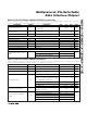
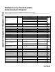
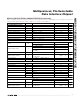
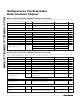
MAX13171E/MAX13173E/MAX13175E Multiprotocol, Pin-Selectable Data Interface Chipset Table 2. MAX13173E Mode Selection PROTOCOL M2 M1 M0 DCE/ DTE INVERT T1 T2 T3 R1 R2 R3 T4 R4 T5 R5 Not Used (Default V.11) 0 0 0 0 0 V.11 V.11 Z V.11 V.11 V.11 Z V.10 Z V.10 RS-530A 0 0 1 0 0 V.11 V.10 Z V.11 V.10 V.11 Z V.10 Z V.10 RS-530 0 1 0 0 0 V.11 V.11 Z V.11 V.11 V.11 Z V.10 Z V.10 X.21 0 1 1 0 0 V.11 V.11 Z V.11 V.11 V.11 Z V.10 Z V.10 V.
Multiprotocol, Pin-Selectable Data Interface Chipset The state of the MAX13175E’s mode-select inputs, M0, M1, M2, and DCE/DTE determines the mode of each of the six termination networks. Table 3 shows a cross-reference of termination mode and select input state for each of the six termination networks within the MAX13175E.
MAX13171E/MAX13173E/MAX13175E Multiprotocol, Pin-Selectable Data Interface Chipset No-Cable Mode The MAX13171E/MAX13173E enter no-cable mode when the mode-select inputs are left unconnected or connected high (M0 = M1 = M2 = 1). The receiver outputs enter a high-impedance state in no-cable mode, allowing these output lines to be shared with other receiver outputs (the receiver outputs have an internal pullup resistor to pull the outputs high if not driven).
Multiprotocol, Pin-Selectable Data Interface Chipset MAX13171E/MAX13173E/MAX13175E 100pF VCC 100pF 100pF VCC C4 4.7µF VL 0.1µF 0.1µF VDD MAX13175E DTE_TXD/DCE_RXD T1IN DTE_SCTE/DCE_RXC T2IN T3IN DTE_TXC/DCE_TXC R1OUT DTE_RXC/DCE_SCTE R2OUT DTE_RXD/DCE_TXD R3OUT VL T1 T2 NC VL DTE 2 TXD A 14 TXD B 24 SCTE A 11 SCTE B DCE RXD A RXD B RXC A RXC B T3 R1 R2 R3 T3OUTA/R1INA T3OUTB/R1INB R2INA R2INB R3INA R3INB 15 12 17 9 3 16 7 MAX13171E M0 M1 M2 0.1µF R6A R6B 0.
MAX13171E/MAX13173E/MAX13175E Multiprotocol, Pin-Selectable Data Interface Chipset UNBALANCED INTERCONNECTING CABLE GENERATOR LOAD CABLE TERMINATION A A′ C C′ RECEIVER Figure 18. Typical V.10/V.28 Interface IZ -10V +3.25mA -3V VZ +10V +3V -3.25mA Figure 19. Receiver Input Impedance Curve A′ A′ A R8 5kΩ A MAX13171E MAX13173E R5 55kΩ R8 5kΩ R6 11kΩ MAX13173E R5 55kΩ RECEIVER S3 R6 11kΩ RECEIVER S3 + 1.4V R7 11kΩ B′ R4 55kΩ B S1 S2 C′ GND Figure 20a. V.
Multiprotocol, Pin-Selectable Data Interface Chipset tem noise, the MAX13171E/MAX13173E V.11 receivers have a typical hysteresis of 15mV. Switch S3 in Figure 23 is open in V.11 mode to disable the V.28 5kΩ termination at the inverting receiver input. Because the control signals are slow (60kbps), 100Ω termination resistance is generally not required for the MAX13173E. For high-speed data transmission, the V.11 specification recommends terminating the cable at the receiver with a 100Ω resistor.
MAX13171E/MAX13173E/MAX13175E Multiprotocol, Pin-Selectable Data Interface Chipset V.28 (RS-232) Interface The V.28 interface is an unbalanced single-ended interface (Figure 18). The V.28 driver generates a minimum of ±5V across the 3kΩ load impedance between A’ and C’. The V.28 receiver has a single-ended input. The MAX13171E/MAX13173E V.28 mode receivers have a threshold between +0.8V and +2.0V. To aid in rejecting system noise, the MAX13171E/MAX13173E V.28 receivers have a typical hysteresis of 250mV.
Multiprotocol, Pin-Selectable Data Interface Chipset 50Ω LOAD CABLE TERMINATION A′ A MAX13171E/MAX13173E/MAX13175E BALANCED INTERCONNECTING CABLE GENERATOR 125Ω RECEIVER 50Ω 125Ω 50Ω 50Ω B B′ C C′ GND GND Figure 25. Typical V.35 Interface A A′ MAX13171E R5 55kΩ R1 52Ω R8 5kΩ MAX13175E RECEIVER S3 S1 S2 R6 11kΩ R3 127Ω + 1.4V R7 11kΩ R2 52Ω B′ R4 55kΩ B S1 S2 C′ GND Figure 26. V.
MAX13171E/MAX13173E/MAX13175E Multiprotocol, Pin-Selectable Data Interface Chipset 100pF VCC 100pF 100pF VCC C4 4.7µF VL 0.1µF 0.
Multiprotocol, Pin-Selectable Data Interface Chipset MAX13171E/MAX13173E/MAX13175E 100pF VCC 100pF 100pF VCC C4 4.7µF VL 0.1µF 0.1µF VDD MAX13175E RXD T1IN RXC T2IN T3IN TXC R1OUT SCTE R2OUT TXD R3OUT VL 0.1µF NC C4 4.7µF T1 T2 R6A R6B R5A R5B 0.1µF T1OUTA T1OUTB T2OUTA T2OUTB R4A R4B C5 4.7µF VEE VL M0 LATCH VEE R2A R2B R3A R3B C3 4.7µF CHARGE PUMP R1A R1B VDD 0.
MAX13171E/MAX13173E/MAX13175E Multiprotocol, Pin-Selectable Data Interface Chipset 100pF VCC 100pF 100pF VCC C4 4.7µF VL 0.1µF 0.1µF VDD MAX13175E TXD T1IN SCTE T2IN T3IN TXC R1OUT RXC R2OUT RXD R3OUT VL T1 T2 M0 DTE 2 TXD A (103) 14 TXD B 24 SCTE A (113) 11 SCTE B T3 R1 R2 R3 T3OUTA/R1INA T3OUTB/R1INB R2INA R2INB R3INA R3INB 15 12 17 9 3 14 7 MAX13171E M0 M1 M2 DCE/DTE 0.1µF R6A R6B 0.1µF T1OUTA T1OUTB T2OUTA T2OUTB R5A R5B VEE R4A R4B C5 4.
Multiprotocol, Pin-Selectable Data Interface Chipset extra protection against static electricity. Maxim’s engineers have developed state-of-the-art structures to protect these pins against ESD of ±15kV without damage. The ESD structures withstand high ESD in all states: normal operation, shutdown, and powered down. After an ESD event, the MAX13171E/MAX13173E/MAX13175E keep working without latchup or damage. ESD protection can be tested in various ways.
ESD Test Conditions ESD performance depends on a variety of conditions. Contact Maxim for a reliability report that documents test setup, test methodology, and test results. Human Body Model Figure 31a shows the Human Body Model, and Figure 31b shows the current waveform it generates when discharged into a low impedance. This model consists of a 100pF capacitor charged to the ESD voltage of interest, which is then discharged into the test device through a 1.5kΩ resistor.
Multiprotocol, Pin-Selectable Data Interface Chipset N.C. N.C. GND T1OUTA T1OUTB T2OUTA T2OUTB GND T3OUTA/R1INA T3OUTB/R1INB R2INA R2INB TOP VIEW 31 30 29 28 27 26 25 24 23 22 21 20 VEE 32 19 GND C2- 33 18 R3INA C2+ 34 17 R3INB MAX13171E GND 35 16 VCC 15 DCE/DTE C1- 36 C1+ 37 + VCC T1IN T2IN N.C. 7 8 9 10 11 12 VL 6 M0 5 R3OUT 4 R2OUT 3 R1OUT 2 T3IN 1 N.C. 13 M1 N.C.
Pin Configurations (continued) R6B R6B R6A R6A R5A R5A R5B R5B R4A R4A R4B R4B TOP VIEW 31 30 29 28 27 26 25 24 23 22 21 20 DCE/DTE 32 19 VCC LATCH 33 18 GND M2 34 17 VDD MAX13175E M1 35 16 VEE M0 36 15 VL R1C 37 + 1 2 3 4 5 6 7 8 9 10 11 12 R1A R2A R2A R2B R2B R2C R3A R3A R3B R3B 13 GND R1A R1B 38 14 R3C *EP R1B MAX13171E/MAX13173E/MAX13175E Multiprotocol, Pin-Selectable Data Interface Chipset TQFN *CONNECT EXPOSED PAD TO VEE Package Info