
User Manual

MAX13171E/MAX13173E/MAX13175E
Multiprotocol, Pin-Selectable
Data Interface Chipset
2 _______________________________________________________________________________________
ABSOLUTE MAXIMUM RATINGS
MAX13171E ELECTRICAL CHARACTERISTICS
(V
CC
= +3.135V to +5.5V, V
L
= +1.62V to +5.5V, C1 = C2 = 1µF, C3 = C4 = C5 = 4.7µF (Figure 15), T
A
= -40°C to +85°C, unless oth-
erwise noted. Typical values are at V
CC
= +3.3V, V
L
= +1.8V, T
A
= +25°C.) (Note 2)
Stresses beyond those listed under “Absolute Maximum Ratings” may cause permanent damage to the device. These are stress ratings only, and functional
operation of the device at these or any other conditions beyond those indicated in the operational sections of the specifications is not implied. Exposure to
absolute maximum rating conditions for extended periods may affect device reliability.
Note 1: Package thermal resistances were obtained using the method described in JEDEC specification JESD51-7, using a four-layer
board. For detailed information on package thermal considerations, refer to http://www.maxim-ic.com/thermal-tutorial
.
(All voltages to GND, unless otherwise noted.)
Supply Voltages
V
CC
........................................................................ -0.3V to +6V
V
L
........................................................................... -0.3V to +6V
V
EE
..................................................................... +0.3V to -7.1V
V
DD
.................................................................... -0.3V to +7.1V
V
DD
to V
CC
............................................................-0.3V to +6V
Logic-Input Voltages
M0, M1, M2, DCE/DTE, LATCH, INVERT, T_IN ..... -0.3V to +6V
Termination Network Inputs
R_A, R_B, R_C.......................................................-15V to +15V
R_A to R_B (only for high-Z state) .....................................±14V
R_A to R_B...........................................................................±6V
R_A to R_C (only for high-Z state) .....................................±14V
R_A to R_C...........................................................................±3V
R_B to R_C (only for high-Z state) .......................................±3V
Logic-Output Voltages
R_OUT ........................................................-0.3V to (V
L
+ 0.3V)
Transmitter Outputs
T_OUT_, T_OUT_/R_IN_
(no-cable, V.28, V.10 modes) ...............................-15V to +15V
Short-Circuit Duration to GND..................................Continuous
Receiver Inputs
R_IN_, T_OUT_/R_IN ............................................-15V to +15V
R_INA to R_INB, T3OUTA/R3INA
to T3OUTB/R3INB ................................................-15V to +15V
Continuous Power Dissipation (T
A
= +70°C)
38-Pin TQFN (derate 35.7mW/°C above +70°C) ........2857mW
Junction-to-Case Thermal Resistance (θ
JC
) (Note 1)
38-Pin TQFN ....................................................................1°C/W
Junction-to-Ambient Thermal Resistance (θ
JA
) (Note 1)
38-Pin TQFN ..................................................................28°C/W
Operating Temperature Range ...........................-40°C to +85°C
Junction Temperature......................................................+150°C
Storage Temperature Range ............................-65°C to +150°C
Lead Temperature (soldering, 10s) ................................+300°C
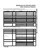
PARAMETER SYMBOL CONDITIONS MIN TYP MAX UNITS
V
CC
Operating Range V
CC
3.135 5.5 V
V
L
Operating Range V
L
1.62 V
CC
V
V
L
Supply Current I
L
All inputs connected to GND, all receiver
outputs low, V
L
= +5.5V
550 800 µA
RS-530, RS-530A, X.21, V.36/RS-449
mode (V.11), no load
15 28 mA
RS-530, RS-530A, X.21, V.36/RS-449
mode (V.11), full load
150 200 mA
V.35 mode, no load 21 38 mA
V.35 mode, full load 150 210 mA
V.28 mode, no load 15 30 mA
V.28 mode, full load 28 42 mA
V
CC
Supply Current (DCE Mode)
(Digital Inputs = GND or V
CC
)
(Transmitter Outputs Static)
I
CC
No-cable mode 0.01 10 µA
RS-530, RS-530A, X.21, V.36/RS-449
mode (V.11), full load
100
V.35 mode, full load 500
Internal Power Dissipation
(DCE Mode)(Static)
P
D
V.28 mode, full load 70
mW