
User Manual

MAX13171E/MAX13173E/MAX13175E
Multiprotocol, Pin-Selectable
Data Interface Chipset
_______________________________________________________________________________________ 9
Note 2: All devices are 100% production tested at T
A
= +85°C for the MAX13171E/MAX13173E and T
A
= +25°C for the
MAX13175E. Specifications over temperature are guaranteed by design.
Note 3: Guaranteed by design, not production tested.
Note 4: Output-to-output skews are evaluated as difference of propagation delays between different channels in the same condition
and for the same polarity (LH or HL).
Note 5: M[x] is the input bus DTE/DCE, M2, M1, M0.
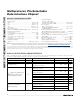
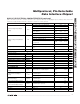
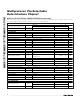
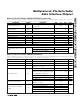
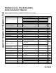
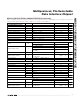
MAX13175E ELECTRICAL CHARACTERISTICS (continued)
(V
CC
= +3.135V to +5.5V, V
L
= +1.62V to +5.5V, C1 = C2 = 1µF, C3 = C4 = C5 = 4.7µF, Figure 15, T
A
= -40°C to +85°C, unless
otherwise noted. Typical values are at V
CC
= +3.3V, V
L
= +1.8V, T
A
= +25°C.) (Note 2)
PARAMETER SYMBOL CONDITIONS MIN TYP MAX UNITS
-7V ≤ V
CM
≤ +7V, all channels, except no-
cable mode, Figure 12
100 104 110
Differential-Mode Impedance
V.11 Mode
-7V ≤ V
CM
≤ +7V, no cable, V
EE
= 0V,
V
AB
< 2V, Figure 12
115
Ω
Differential Path Enable Time 50 µs
Differential Path Disable Time 300 µs
Common-Mode Path Enable Time 12 µs
Common-Mode Path Disable
Time
2µs
High-Impedance Leakage
Current
I
Z
-15V ≤ V
R_A
≤ +15V -50 +50 µA
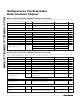
LOGIC INPUTS (M0, M1, M2, LATCH, DCE/DTE)
Input High Voltage V
IH
0.66 x V
L
V
Input Low Voltage V
IL
0.33 x V
L
V
Logic Input Current I
IN
V
IN
= GND or V
L
-1 +1 µA
ESD PROTECTION
Human Body Model ±15
Air Gap Discharge IEC 61000-4-2 ±10R_A, R_B to GND
Contact Discharge IEC 61000-4-2 ±6
kV
All Other Pins Human Body Model ±2 kV