9-3151; Rev 0; 4/04 14-Bit, 4-Channel, Software-Programmable, Multiranging, Simultaneous-Sampling ADC The MAX1338 14-bit, analog-to-digital converter (ADC) offers four simultaneously sampled, fully differential input channels, with independent track-and-hold (T/H) circuitry for each channel. The input channels are individually software programmable for input ranges of ±10V, ±5V, ±2.5V, and ±1.25V. The input channels feature fault tolerance to ±17V.
MAX1338 14-Bit, 4-Channel, Software-Programmable, Multiranging, Simultaneous-Sampling ADC ABSOLUTE MAXIMUM RATINGS CS, RD, WR, CONVST, to DRGND........-0.3V to (DRVDD + 0.3V) SHDN, STANDBY, CLK, EOC, EOLC to DRGND ................................-0.3V to (DRVDD + 0.3V) Maximum Current into Any Pin .........................................±50mA Continuous Power Dissipation (TA = +70°C) 56-Pin Thin QFN (derate 31.3mW /°C above +70°C)....2500mW Operating Temperature Range ...........................
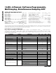
14-Bit, 4-Channel, Software-Programmable, Multiranging, Simultaneous-Sampling ADC (AVDD = DVDD = +5.0V, DRVDD = +3.0V, AGND = DGND = DRGND = 0, INTCLK/EXTCLK = AGND, fCLK = 5MHz, input range = ±10V, REFP2 = REFP1, REFN2 = REFN1, COM1 = COM2, 1.0nF from REFADC to AGND, 1.0µF and 0.1µF from COM1 to AGND, 0.1µF from REFP1 to AGND, 0.1µF from REFN1 to AGND, 1.0µF from REFP1 to REFN1. Typical values are at TA = +25°C. TA = TMIN to TMAX, unless otherwise noted.
MAX1338 14-Bit, 4-Channel, Software-Programmable, Multiranging, Simultaneous-Sampling ADC ELECTRICAL CHARACTERISTICS (continued) (AVDD = DVDD = +5.0V, DRVDD = +3.0V, AGND = DGND = DRGND = 0, INTCLK/EXTCLK = AGND, fCLK = 5MHz, input range = ±10V, REFP2 = REFP1, REFN2 = REFN1, COM1 = COM2, 1.0nF from REFADC to AGND, 1.0µF and 0.1µF from COM1 to AGND, 0.1µF from REFP1 to AGND, 0.1µF from REFN1 to AGND, 1.0µF from REFP1 to REFN1. Typical values are at TA = +25°C. TA = TMIN to TMAX, unless otherwise noted.
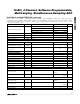
14-Bit, 4-Channel, Software-Programmable, Multiranging, Simultaneous-Sampling ADC (AVDD = DVDD = +5.0V, DRVDD = +3.0V, AGND = DGND = DRGND = 0, INTCLK/EXTCLK = AGND, fCLK = 5MHz, input range = ±10V, REFP2 = REFP1, REFN2 = REFN1, COM1 = COM2, 1.0nF from REFADC to AGND, 1.0µF and 0.1µF from COM1 to AGND, 0.1µF from REFP1 to AGND, 0.1µF from REFN1 to AGND, 1.0µF from REFP1 to REFN1. Typical values are at TA = +25°C. TA = TMIN to TMAX, unless otherwise noted.) PARAMETER SYMBOL CONDITIONS MIN TYP MAX 2.
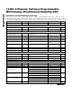
MAX1338 14-Bit, 4-Channel, Software-Programmable, Multiranging, Simultaneous-Sampling ADC ELECTRICAL CHARACTERISTICS (continued) (AVDD = DVDD = +5.0V, DRVDD = +3.0V, AGND = DGND = DRGND = 0, INTCLK/EXTCLK = AGND, fCLK = 5MHz, input range = ±10V, REFP2 = REFP1, REFN2 = REFN1, COM1 = COM2, 1.0nF from REFADC to AGND, 1.0µF and 0.1µF from COM1 to AGND, 0.1µF from REFP1 to AGND, 0.1µF from REFN1 to AGND, 1.0µF from REFP1 to REFN1. Typical values are at TA = +25°C. TA = TMIN to TMAX, unless otherwise noted.
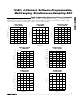
14-Bit, 4-Channel, Software-Programmable, Multiranging, Simultaneous-Sampling ADC (AVDD = DVDD = +5.0V, DRVDD = +3.0V, AGND = DGND = DRGND = 0, INTCLK/EXTCLK = AGND, fCLK = 5MHz, input range = ±10V, REFP2 = REFP1, REFN2 = REFN1, COM1 = COM2, 1.0nF from REFADC to AGND, 1.0µF and 0.1µF from COM1 to AGND, 0.1µF from REFP1 to AGND, 0.1µF from REFN1 to AGND, 1.0µF from REFP1 to REFN1.) INTEGRAL NONLINEARITY vs. OUTPUT CODE OFFSET ERROR vs. SUPPLY VOLTAGE DIFFERENTIAL NONLINEARITY vs. OUTPUT CODE 0.
Typical Operating Characteristics (continued) (AVDD = DVDD = +5.0V, DRVDD = +3.0V, AGND = DGND = DRGND = 0, INTCLK/EXTCLK = AGND, fCLK = 5MHz, input range = ±10V, REFP2 = REFP1, REFN2 = REFN1, COM1 = COM2, 1.0nF from REFADC to AGND, 1.0µF and 0.1µF from COM1 to AGND, 0.1µF from REFP1 to AGND, 0.1µF from REFN1 to AGND, 1.0µF from REFP1 to REFN1.) SIGNAL-TO-NOISE RATIO vs.
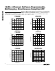
14-Bit, 4-Channel, Software-Programmable, Multiranging, Simultaneous-Sampling ADC (AVDD = DVDD = +5.0V, DRVDD = +3.0V, AGND = DGND = DRGND = 0, INTCLK/EXTCLK = AGND, fCLK = 5MHz, input range = ±10V, REFP2 = REFP1, REFN2 = REFN1, COM1 = COM2, 1.0nF from REFADC to AGND, 1.0µF and 0.1µF from COM1 to AGND, 0.1µF from REFP1 to AGND, 0.1µF from REFN1 to AGND, 1.0µF from REFP1 to REFN1.) SUPPLY CURRENT vs. SUPPLY VOLTAGE DRIVER SUPPLY CURRENT vs. SUPPLY VOLTAGE SUPPLY CURRENT vs.
Typical Operating Characteristics (continued) (AVDD = DVDD = +5.0V, DRVDD = +3.0V, AGND = DGND = DRGND = 0, INTCLK/EXTCLK = AGND, fCLK = 5MHz, input range = ±10V, REFP2 = REFP1, REFN2 = REFN1, COM1 = COM2, 1.0nF from REFADC to AGND, 1.0µF and 0.1µF from COM1 to AGND, 0.1µF from REFP1 to AGND, 0.1µF from REFN1 to AGND, 1.0µF from REFP1 to REFN1.) SHUTDOWN CURRENT vs. TEMPERATURE STANDBY CURRENT vs. SUPPLY VOLTAGE SHDN = AVDD 65 STANDBY = AVDD 4.25 4.20 A|DD (mA) 55 4.15 50 4.10 45 4.05 40 4.
14-Bit, 4-Channel, Software-Programmable, Multiranging, Simultaneous-Sampling ADC PIN NAME FUNCTION 1, 7, 9, 17, 19 AVDD Analog Power Input. AVDD is the power input for the analog section of the converter. Connect a +4.75V to +5.25V power supply to AVDD. Bypass each AVDD to AGND with a 0.1µF capacitor very close to the device. Bypass AVDD to AGND with a bulk capacitor of at least 4.7µF where power enters the board. Connect all AVDD pins to the same potential.
14-Bit, 4-Channel, Software-Programmable, Multiranging, Simultaneous-Sampling ADC MAX1338 Pin Description (continued) PIN NAME FUNCTION 41 D12 Data Output Bit 12 42 D13 Data Output Bit 13 (MSB) 43 DRVDD Digital I/O Power-Supply Input. DRVDD is the power input for the digital I/O buffers and drivers. Connect a +2.7V to +5.25V power supply to DRVDD. Bypass DRVDD to DRGND with a 0.1µF capacitor very close to the device. 44 DRGND Driver Ground. DRGND is the power-supply return for DRVDD.
14-Bit, 4-Channel, Software-Programmable, Multiranging, Simultaneous-Sampling ADC MAX1338 DVDD DRVDD AVDD AIN0+ MAX1338 D13 S/H AIN0- 4x1 MUX AIN3+ 14-BIT ADC S/H 4 x 14 SRAM OUTPUT DRIVERS D8 D7 AIN3D0 REFP2 REFP1 COM2 COM1 CONFIGURATION REGISTER REFN2 REFN1 INTERFACE AND CONTROL WR CS RD CONVST SHDN CLK 5kΩ REFADC STANDBY 2.500V EOC EOLC INTCLK/EXTCLK AGND DRGND DGND Figure 2. Functional Diagram Power-Supply Inputs Three separate power supplies power the MAX1338.
MAX1338 14-Bit, 4-Channel, Software-Programmable, Multiranging, Simultaneous-Sampling ADC Figure 3 shows the equivalent analog input T/H circuit for one analog input. As conversion begins, the T/H circuits hold the analog signals. After the 12th clock cycle (or 2.4µs in internal clock mode) into the conversion process, the last analog input sample begins shifting through the converter, and the T/H circuits begin to track the analog inputs again in preparation for the next CONVST rising edge.
14-Bit, 4-Channel, Software-Programmable, Multiranging, Simultaneous-Sampling ADC Applications Sections Power-On Reset At power-up, all channels default to a ±10V input range. After applying power, allow a 1ms wake-up time to elapse and perform one dummy conversion before initiating first conversion. Power Saving Full Shutdown During shutdown, the analog and digital circuits in the MAX1338 power down and the device draws less than 0.06mA from AVDD, and less than 10µA from DVDD.
MAX1338 14-Bit, 4-Channel, Software-Programmable, Multiranging, Simultaneous-Sampling ADC SAMPLE tCONVST CONVST 17 CLK 18 tEOC1 19 20 21 22 24 23 25 26 29 27 tNEXT EOC tEOC EOLC tQUIET RD tACC tRDL D0–D13 CH0 CH1 CH2 CH3 tREQ Figure 5. Reading During a Conversion—Internal or External Clock Starting a Conversion Reading a Conversion Result Internal Clock For internal clock operation, force INTCLK/EXTCLK high.
14-Bit, 4-Channel, Software-Programmable, Multiranging, Simultaneous-Sampling ADC MAX1338 SAMPLE tCONVST CONVST tCLKH tCNTC 27 26 2 1 28 31 30 29 CLK tCLK EOC tCLKL ONLY LAST PULSE SHOWN tEOC EOLC tRTC CS tCTR tQUIET tRDH tRDL RD tEOCRD tEOLCRD D0–D13 CH0 tACC CH1 CH2 CH3 tREQ Figure 6. Reading After a Conversion—External Clock onto the bus. After reading all four channels, bring CS high to release the parallel I/O.
8 x VREFADC INITIAL TRANSFER FUNCTION ADJUSTED TRANSFER FUNCTION 0x0000 MAXIMUM 64 CODES 0x2000 -8192 +8191 0 Figure 7. Example of Digitally Adjusted Transfer Function— Shifted Down to Minimize Zero-Code Offset Input Range Settings Table 4 shows the two’s complement output for a selection of inputs. The full-scale input range (FSR) depends on the selected range, and the voltage at REF, as shown in Table 5. Also shown in Table 5 are the allowable common-mode ranges for the differential inputs.
14-Bit, 4-Channel, Software-Programmable, Multiranging, Simultaneous-Sampling ADC INPUT VOLTAGE (V) ±10V INPUT RANGE SELECTED ±5V INPUT RANGE SELECTED ±2.5V INPUT RANGE SELECTED ±1.25V INPUT RANGE SELECTED DECIMAL EQUIVALENT OUTPUT (CODE10) 9.9988 4.9994 2.4998 1.2499 8191 01 1111 1111 1111 → 0x1FFF 9.9976 4.9988 2.4997 1.2498 8190 01 1111 1111 1110 → 0x1FFE 0.0012 0.0006 0.0002 0.
MAX1338 14-Bit, 4-Channel, Software-Programmable, Multiranging, Simultaneous-Sampling ADC 2 x VREFADC TWO'S COMPLEMENT BINARY OUTPUT CODE TWO'S COMPLEMENT BINARY OUTPUT CODE 4 x VREFADC 0x1FFF 0x1FFE 0x1FFD 0x1FFC 0x0001 0x0000 0x3FFF 0x2003 0x2002 0x2001 0x2000 4 x VREF 1 LSB = -1 -8192 -8190 0 +1 214 0x1FFF 0x1FFE 0x1FFD 0x1FFC 0x0001 0x0000 0x3FFF 0x2003 0x2002 0x2001 0x2000 +8189 +8191 1 LSB = -1 -8192 -8190 INPUT VOLTAGE (VAIN_+ - VAIN_- IN LSBs) 0 +1 2 x VREF 214 +8189 +8191 IN
14-Bit, 4-Channel, Software-Programmable, Multiranging, Simultaneous-Sampling ADC Signal-to-Noise Plus Distortion (SINAD) SINAD indicates the converter’s noise and distortion performance. SINAD is computed by taking the ratio of the RMS signal to the RMS noise plus distortion. RMS noise plus distortion includes all spectral components to the Nyquist frequency excluding the fundamental and the DC offset.
14-Bit, 4-Channel, Software-Programmable, Multiranging, Simultaneous-Sampling ADC MAX1338 Typical Operating Circuit 15 DVDD INTCLK/EXTCLK 54 +5V +5V 0.1µF 1 0.1µF 7 AVDD AVDD 0.1µF 9 AVDD 0.1µF 17 MAX1338 DGND SHDN CLK CONVST AVDD CS 0.1µF 19 0.1µF 21 0.001µF 22 0.1µF 23 AVDD REFADC REFP1 REFP2 WR RD EOLC EOC STANDBY 55, 56 GND 53 51 50 49 48 CONTROL I/O 47 46 45 52 1.0µF 27 0.1µF REFN2 24 25 0.
14-Bit, 4-Channel, Software-Programmable, Multiranging, Simultaneous-Sampling ADC CS RD EOLC EOC DRGND DRVDD 47 46 45 44 43 CONVST 50 WR CLK 51 48 STANDBY 52 49 DVDD SHDN 53 55 54 DGND DGND 56 TOP VIEW TRANSISTOR COUNT: 27,000 PROCESS: BiCMOS EXPOSED PAD: Connect to AGND AVDD 1 42 D13 AIN0+ 2 41 D12 AIN0- 3 40 D11 AIN1+ 4 39 D10 AIN1- 5 38 D9 AGND 6 37 D8 AVDD 7 36 D7 AGND 8 35 D6 MAX1338 23 24 25 26 27 28 COM1 COM2 REFN1 REFN2 AGND
Package Information (The package drawing(s) in this data sheet may not reflect the most current specifications. For the latest package outline information, go to www.maxim-ic.com/packages.) 56L THIN QFN.EPS MAX1338 14-Bit, 4-Channel, Software-Programmable, Multiranging, Simultaneous-Sampling ADC Maxim cannot assume responsibility for use of any circuitry other than circuitry entirely embodied in a Maxim product. No circuit patent licenses are implied.