
Manual

MAX1338
14-Bit, 4-Channel, Software-Programmable,
Multiranging, Simultaneous-Sampling ADC
6 _______________________________________________________________________________________
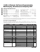
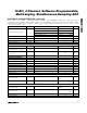
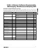
ELECTRICAL CHARACTERISTICS (continued)
(AV
DD
= DV
DD
= +5.0V, DRV
DD
= +3.0V, AGND = DGND = DRGND = 0, INTCLK/EXTCLK = AGND, f
CLK
= 5MHz, input range =
±10V, REFP2 = REFP1, REFN2 = REFN1, COM1 = COM2, 1.0nF from REFADC to AGND, 1.0µF and 0.1µF from COM1 to AGND,
0.1µF from REFP1 to AGND, 0.1µF from REFN1 to AGND, 1.0µF from REFP1 to REFN1. Typical values are at T
A
= +25°C. T
A
= T
MIN
to T
MAX
, unless otherwise noted.)
PARAMETER
SYMBOL
CONDITIONS
MIN
TYP
MAX
UNITS
EOC Fall to RD Fall Setup Time
t
EOCRD
0ns
EOLC Fall to RD Fall Setup Time t
EOLCRD
0ns
Input Data Setup Time t
DTW
10 ns
Input Data Hold Time t
WTD
10 ns
External CLK Period t
CLK
166
200 ns
External CLK High Period t
CLKH
Logic sensitive to rising edges 60 ns
External CLK Low Period t
CLKL
Logic sensitive to rising edges 60 ns
External Clock Frequency f
CLK
(Note 4) 1 6
MHz
Internal Clock Frequency f
INT
5.0
5.25
5.5
MHz
CONVST High to CLK Edge t
CNTC
30 ns
Quiet Time t
QUIET
600
ns
Note 1: See definition for this parameter in the Definitions section.
Note 2: Differential reference voltage (REFP–REFN) error nulled.
Note 3: This is the load the MAX1338 presents to an external reference at REFADC.
Note 4: Minimum CLK frequency is limited only by the internal T/H droop rate. Limit the time between the rising edge of CONVST to
the falling edge of EOLC to a maximum of 0.25ms.
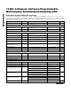
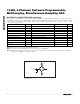
1.6V
1.6mA
0.8mA
50pF
TO OUTPUT PIN
Figure 1. Load Circuit for Data Access Time and Bus-
Relinquish Time