
Owner's manual


MAX1449
10-Bit, 105Msps, Single +3.3V, Low-Power
ADC with Internal Reference
12 ______________________________________________________________________________________
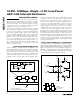
data is valid on the rising edge of the input clock. The
output data has an internal latency of 5.5 clock cycles.
Figure 6 also determines the relationship between the
input clock parameters and the valid output data.
Applications Information
Figure 7 depicts a typical application circuit containing a
single-ended to differential converter. The internal refer-
ence provides a V
DD
/2 output voltage for level shifting
purposes. The input is buffered and then split to a volt-
age follower and inverter. A low-pass filter, to suppress
some of the wideband noise associated with high-speed
op amps, follows the op amps. The user may select the
R
ISO
and C
IN
values to optimize the filter performance, to
suit a particular application. For the application in Figure
7, a R
ISO
of 50Ω is placed before the capacitive load to
prevent ringing and oscillation. The 22pF C
IN
capacitor
acts as a small bypassing capacitor.
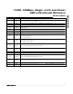
50
58
74
66
82
90
35 4942 56 63 70
CLOCK DUTY CYCLE (%)
SFDR (dBc)
f
IN
= 25.123MHz AT -0.5dB FS
Figure 3a. Spurious Free Dynamic Range vs. Clock Duty
Cycle (Differential Input)
54
57
56
55
60
58
59
61
62
35 4942 56 63 70
CLOCK DUTY CYCLE (%)
SNR (dB)
f
IN
= 25.123MHz AT -0.5dB FS
Figure 3b. Signal-to-Noise Ratio vs. Clock Duty Cycle
(Differential Input)
-85
-75
-80
-65
-70
-55
-60
-50
35 4942 56 63 70
CLOCK DUTY CYCLE (%)
THD (dBc)
f
IN
= 25.123MHz AT -0.5dB FS
Figure 4a. Total Harmonic Distortion vs. Clock Duty Cycle
(Differential Input)
52
56
54
60
58
62
64
35 4942 56 63 70
CLOCK DUTY CYCLE (%)
SINAD (dB)
f
IN
= 25.123MHz AT -0.5dB FS
Figure 4b. Signal-to-Noise Plus Distortion vs. Clock Duty Cycle
(Differential Input)