
Owner's manual


MAX1449
10-Bit, 105Msps, Single +3.3V, Low-Power
ADC with Internal Reference
______________________________________________________________________________________ 13
Using Transformer Coupling
An RF transformer (Figure 8) provides an excellent
solution to convert a single-ended source signal to a
fully differential signal, required by the MAX1449 for
optimum performance. Connecting the center tap of the
transformer to COM provides a V
DD
/2 DC level shift to
the input. Although a 1:1 transformer is shown, a step-
up transformer may be selected to reduce the drive
requirements. A reduced signal swing from the input
driver, such as an op amp, may also improve the over-
all distortion.
In general, the MAX1449 provides better SFDR and
THD with fully differential input signals than single-
ended drive, especially for very high input frequencies.
In differential input mode, even-order harmonics are
lower as both inputs (IN+, IN-) are balanced, and each
of the inputs only requires half the signal swing com-
pared to single-ended mode.
Single-Ended AC-Coupled Input Signal
Figure 9 shows an AC-coupled, single-ended applica-
tion. The MAX4108 op amp provides high speed, high
bandwidth, low-noise, and low-distortion to maintain the
integrity of the input signal.
Grounding, Bypassing
and Board Layout
The MAX1449 requires high-speed board layout design
techniques. Locate all bypass capacitors as close to
the device as possible, preferably on the same side as
the ADC, using surface mount devices for minimum
inductance. Bypass V
DD
, REFP, REFN, and COM with
two parallel 0.1µF ceramic capacitors and a 2.2µF
bipolar capacitor to GND. Follow the same rules to
bypass the digital supply (OV
DD
) to OGND. Multi-layer
boards with separated ground and power planes pro-
duce the highest level of signal integrity. Consider
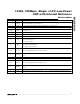
OUTPUT
DATA D9–D0
OE
t
DISABLE
t
ENABLE
HIGH-ZHIGH-Z
VALID DATA
Figure 5. Output Enable Timing
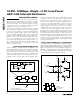
N - 6
N
N - 5
N + 1
N - 4
N + 2
N - 3
N + 3
N - 2
N + 4
N - 1
N + 5
N
N + 6
N + 1
5.5 CLOCK-CYCLE LATENCY
ANALOG INPUT
CLOCK INPUT
DATA OUTPUT
t
D0
t
CH
t
CL
Figure 6. System and Output Timing Diagram