
Owner's manual


MAX1449
10-Bit, 105Msps, Single +3.3V, Low-Power
ADC with Internal Reference
_______________________________________________________________________________________ 3
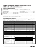
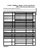
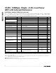
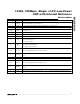
PARAMETER SYMBOL CONDITIONS MIN TYP MAX UNITS
f
IN
= 7.5MHz -72
f
IN
= 20MHz -72
Third-Harmonic Distortion
(Note 1)
HD3
f
IN
= 50MHz -70
dBc
Intermodulation Distortion (First 5
Odd-Order IMDs) (Note 2)
IMD
f
1
= 38MHz at -6.5dB FS
f
2
= 42MHz at -6.5dB FS
-76 dBc
Third-Order Intermodulation
Distortion (Note 2)
IM3
f
1
= 38MHz at -6.5dB FS
f
2
= 42MHz at -6.5dB FS
-76 dBc
f
IN
= 7.5MHz, T
A
= +25°C -70 -61.5
f
IN
= 20MHz, T
A
= +25°C -70 -61.5 dBc
Total Harmonic Distortion
(First 5 Harmonics)
(Note 1)
THD
f
IN
= 50MHz -70
Small-Signal Bandwidth Input at -20dB FS, differential inputs 500 MHz
Full-Power Bandwidth FPBW Input at -0.5dB FS, differential inputs 400 MHz
Aperture Delay t
AD
1ns
Aperture Jitter t
AJ
2ps
RMS
Overdrive Recovery Time For 1.5 x full-scale input 2 ns
Differential Gain ±1%
Differential Phase ±0.25 degree
Output Noise IN+ = IN- = COM 0.2 LS B
RM S
INTERNAL REFERENCE
Reference Output Voltage REFOUT
2.048
±1%
V
Reference Temperature
Coefficient
TC
REF
60 ppm/° C
Load Regulation 1.25 mV/mA
EXTERNAL REFERENCE
Positive Reference REFP V
REFIN
= +2.048V 2.162 V
Negative Reference REFN V
REFIN
= +2.048V 1.138 V
Differential Reference Voltage ∆V
REF
V
REFP
-V
REFN
, V
REFIN
= +2.048V 0.98 1.024 1.07 V
REFIN Resistance R
REFIN
>50 MΩ
DIGITAL INPUTS (CLK, PD, OE)
CLK
0.8 x
V
DD
Input High Threshold V
IH
PD, OE
0.8 x
V
DD
V
CLK
0.2 x
V
DD
Input Low Threshold V
IL
PD, OE
0.2 x
V
DD
V
ELECTRICAL CHARACTERISTICS (continued)
(V
DD
= +3.3V, OV
DD
= +2.0V; 0.1µF and 1.0µF capacitors from REFP, REFN, and COM to GND; V
REFIN
= +2.048V, REFOUT
connected to REFIN through a 10kΩ resistor, V
IN
= 2Vp-p (differential with respect to COM), C
L
≈ 10pF at digital outputs, f
CLK
=
105MHz, T
A
= T
MIN
to T
MAX
, unless otherwise noted. Typical values are at T
A
=
+25°C.)