
Owner's manual


Note 1: SNR, SINAD, THD, SFDR and HD3 are based on an analog input voltage of -0.5dB FS referenced to a +1.024V full-scale
input voltage range.
Note 2: Intermodulation distortion is the total power of the intermodulation products relative to the individual carrier. This number is
6dB better if referenced to the two-tone envelope.
Note 3: Digital outputs settle to V
IH
,V
IL
.
Note 4: With REFIN driven externally, REFP, COM, and REFN are left floating while powered down.
MAX1449
10-Bit, 105Msps, Single +3.3V, Low-Power
ADC with Internal Reference
4 _______________________________________________________________________________________
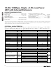
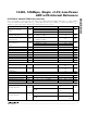
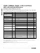
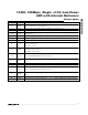
PARAMETER SYMBOL CONDITIONS MIN TYP MAX UNITS
Input Hysteresis V
HYST
0.1 V
I
IH
V
IH
= V
DD
= OV
DD
±5 µA
Input Leakage
I
IL
V
IL
= 0 ±5
Input Capacitance C
IN
5pF
DIGITAL OUTPUTS (D9–D0)
Output Voltage Low V
OL
I
SINK
= 200µA 0.2 V
Output Voltage High V
OH
I
SOURCE
= 200µA
OV
DD
- 0.2
V
Three-State Leakage Current I
LEAK
OE = OV
DD
±10 µA
Three-State Output Capacitance C
OUT
OE = OV
DD
5pF
POWER REQUIREMENTS
Analog Supply Voltage V
DD
2.7 3.3 3.6 V
Output Supply Voltage OV
DD
1.7 3.3 3.6 V
Operating, f
IN
= 20MHz at -0.5dB FS 58 74 mA
Analog Supply Current I
VDD
Shutdown, clock idle, PD = OE = OV
DD
415µA
Operating, C
L
= 15pF , f
IN
= 20MHz at
-0.5dB FS
10 mA
Output Supply Current I
OVDD
Shutdown, clock idle, PD = OE = OV
DD
110µA
Offset ±0.1 mV/V
Power Supply Rejection PSRR
Gain ±0.1 %/V
TIMING CHARACTERISTICS
CLK Rise-to-Output Data Valid t
DO
Figure 6 (Note 3) 5 8 ns
OE Fall-to-Output Enable t
ENABLE
Figure 5 10 ns
OE Rise-to-Output Disable t
DISABLE
Figure 5 15 ns
CLK Pulse Width High t
CH
Figure 6, clock period 9.52ns
4.76
±0.47
ns
CLK Pulse Width Low t
CL
Figure 6, clock period 9.52ns
4.76
±0.47
ns
Wake-Up Time t
WAKE
(Note 4) 1.5 µs
ELECTRICAL CHARACTERISTICS (continued)
(V
DD
= +3.3V, OV
DD
= +2.0V; 0.1µF and 1.0µF capacitors from REFP, REFN, and COM to GND; V
REFIN
= +2.048V, REFOUT
connected to REFIN through a 10kΩ resistor, V
IN
= 2Vp-p (differential with respect to COM), C
L
≈ 10pF at digital outputs,
f
CLK
= 105MHz, T
A
= T
MIN
to T
MAX
, unless otherwise noted. Typical values are at T
A
=
+25°C.)