
Owner's manual
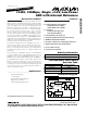


MAX1449
10-Bit, 105Msps, Single +3.3V, Low-Power
ADC with Internal Reference
_______________________________________________________________________________________ 9
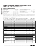
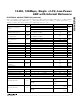
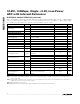
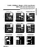
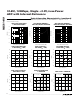
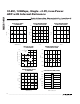
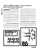
Pin Description
PIN NAME FUNCTION
1 REFN
Lower Reference. Conversion range is ±(V
REFP
- V
REFN
).
Bypass to GND with a > 0.1µF capacitor.
2 COM Common-Mode Voltage Output. Bypass to GND with a > 0.1µF capacitor.
3, 9, 10 V
DD
Analog Supply Voltage. Bypass to GND with a capacitor combination of 2.2µF in parallel with 0.1µF.
4, 5, 8, 11,
14, 30
GND Analog Ground
6 IN+ Positive Analog Input. For single-ended operation connect signal source to IN+.
7 IN- Negative Analog Input. For single-ended operation connect IN- to COM.
12 CLK Conversion Clock Input
13 PD
Power Down Input.
High: Power-down mode
Low: Normal operation
15 OE
Output Enable Input.
High: Digital outputs disabled
Low: Digital outputs enabled
16–20 D9–D5 Three-State Digital Outputs D9–D5. D9 is the MSB.
21 OV
DD
Output Driver Supply Voltage. Bypass to GND with a capacitor combination of 2.2µF in parallel with
0.1µF.
22 T.P. Test Point. Do not connect.
23 OGND Output Driver Ground
24–28 D4–D0 Three-State Digital Outputs D4–D0. D0 is the LSB.
29 REFOUT
Internal Reference Voltage Output. May be connected to REFIN through a resistor or a resistor-
divider.
31 REFIN Reference Input. V
REFIN
= 2
✕
(V
REFP
- V
REFN
). Bypass to GND with a > 0.1µF capacitor.
32 REFP Upper Reference. Conversion range is ±(V
REFP
- V
REFN
). Bypass to GND with a > 0.1µF capacitor.