9-3579; Rev 0; 2/05 Low-Power, Low-Noise Multichannel Sensor Signal Processor Features The MAX1464 is a highly integrated, low-power, lownoise multichannel sensor signal processor optimized for industrial, automotive, and process-control applications such as pressure sensing and compensation, RTD and thermocouple linearization, weight sensing and classification, and remote process monitoring with limit indication.
MAX1464 Low-Power, Low-Noise Multichannel Sensor Signal Processor ABSOLUTE MAXIMUM RATINGS VDD to VSS .............................................................-0.3V to +6.0V VDDF to VSS ...........................................................-0.3V to +6.0V VSSF to VSS ............................................................-0.3V to +0.3V All Other Pins to VSS ...................................-0.3V to (VDD + 0.3V) Continuous Power Dissipation (TA = +70°C) 28-Pin SSOP (derate 9.
Low-Power, Low-Noise Multichannel Sensor Signal Processor (VDDF = VDD = 4.5V to 5.5V, VSSF = VSS = 0V, fCLK = 4.0MHz, TA = TMIN to TMAX. Typical values are at VDDF = VDD = 5.0V, VSSF = VSS = 0V, TA = +25°C, unless otherwise noted.
MAX1464 Low-Power, Low-Noise Multichannel Sensor Signal Processor ELECTRICAL CHARACTERISTICS (continued) (VDDF = VDD = 4.5V to 5.5V, VSSF = VSS = 0V, fCLK = 4.0MHz, TA = TMIN to TMAX. Typical values are at VDDF = VDD = 5.0V, VSSF = VSS = 0V, TA = +25°C, unless otherwise noted.
Low-Power, Low-Noise Multichannel Sensor Signal Processor (VDDF = VDD = 4.5V to 5.5V, VSSF = VSS = 0V, fCLK = 4.0MHz, TA = TMIN to TMAX. Typical values are at VDDF = VDD = 5.0V, VSSF = VSS = 0V, TA = +25°C, unless otherwise noted.) (Note 1) PARAMETER SYMBOL CONDITIONS MIN TYP MAX UNITS VOS_LG 0 ±6 mV IB_LG ±225 nA LARGE OP AMP Input Offset Voltage Input Bias Current DC Gain AVOL_LG OUTnLG = 0.5V to 4.5V (n = 1 or 2), RLOAD = ∞ 100 dB Gain Bandwidth Product GBW_LG AVOL_LG = +1V/V 4.
MAX1464 Low-Power, Low-Noise Multichannel Sensor Signal Processor ELECTRICAL CHARACTERISTICS (continued) (VDDF = VDD = 4.5V to 5.5V, VSSF = VSS = 0V, fCLK = 4.0MHz, TA = TMIN to TMAX. Typical values are at VDDF = VDD = 5.0V, VSSF = VSS = 0V, TA = +25°C, unless otherwise noted.) (Note 1) PARAMETER SYMBOL Bit Weight BWPWM Offset Error VPWM_OS Gain Error GEPWM Output Jitter OJPWM CONDITIONS MIN PWM data = 0000h (Note 7) TYP MAX UNITS 2 µs/LSB ±1 µs ±0.
Low-Power, Low-Noise Multichannel Sensor Signal Processor (VDDF = VDD = 4.5V to 5.5V, VSSF = VSS = 0V, fCLK = 4.0MHz, TA = TMIN to TMAX. Typical values are at VDDF = VDD = 5.0V, VSSF = VSS = 0V, TA = +25°C, unless otherwise noted.) (Note 1) PARAMETER SYMBOL CONDITIONS MIN TYP MAX UNITS DIGITAL INPUTS (GPIO1, GPIO2, SCLK, DI, CKSEL, CKIO, CS) Input High Threshold Voltage VIH Input Low Threshold Voltage VIL Input Hysteresis 0.8 x VDD 0.
MAX1464 Low-Power, Low-Noise Multichannel Sensor Signal Processor TIMING CHARACTERISTICS (VDDF = VDD = 4.5V to 5.5V, VSSF = VSS = 0V, fCLK = 4.0MHz, TA = TMIN to TMAX. Typical values are at VDDF = VDD = 5.0V, VSSF = VSS = 0V, TA = +25°C, unless otherwise noted.) (Note 1) PARAMETER Programming Temperature SYMBOL CONDITIONS MIN TYP TPROG Internal Oscillator Clock Frequency fICLK OSC[4:0] = 00000 External Clock Frequency fECLK VCKSEL = 0 3.3 4.15 Min 0.2 Max 5 MAX UNITS 125 °C 5.
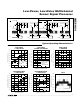
Low-Power, Low-Noise Multichannel Sensor Signal Processor MAX1464 tCS CS tCSI tCSS tCL tSC tCH tCSS tSC tCSH tCL tCH tCSH SCLK tDS tDS tDH tDH DI tDV tDO tTR tDV tDO tTR DO Figure 1. Serial Interface Timing Diagram Typical Operating Characteristics (VDD = 5.0V, TA = +25°C, unless otherwise noted.) SUPPLY CURRENT vs. INTERNAL CLOCK FREQUENCY 2.40 CPU ON 2% OF TIME ADC ON 98% OF TIME ADCCLK = 1MHz DAC1 ON SMALL OP AMP ON 2.35 TA = -40°C 2.30 2.50 2.45 2.
Typical Operating Characteristics (continued) (VDD = 5.0V, TA = +25°C, unless otherwise noted.) DAC INL 1 0 -1 -2 -3 MAX1464 toc08 3 0.03 2 0.02 DAC DNL ERROR (LSB) 2 DAC NONLINEARITY ERROR (%FS) MAX1464 toc07 3 DAC DNL 0.04 MAX1464 toc09 ADC DNL 4 ADC DNL ERROR (LSB) 0.01 0 -0.01 1 0 -1 -0.02 -2 -0.03 PGA[4:0] = 01000 -0.04 -1.0 -0.5 0 0.5 1.0 -3 -0.8 -0.6 -0.4 -0.2 INPUT VOLTAGE NORMALIZED TO FULL SCALE 0 0.2 0.4 0.6 -0.8 -0.6 -0.4 -0.
Low-Power, Low-Noise Multichannel Sensor Signal Processor PIN NAME FUNCTION 1 OUT1SM 2 AMP1M Op Amp 1 Negative Input 3 AMP1P Op Amp 1 Positive Input Small Op Amp 1 Output 4 OUT1LG 5, 7 N.C. No Connection Large Op Amp 1 Output 6 VDD Positive Supply Voltage Input. Bypass VDD to VSS with a 0.1µF ceramic capacitor. 8 CKSEL Clock-Select Digital Input 9 CKIO Clock Digital Input/Output 10 CS SPI Chip-Select Digital Input. Active low.
MAX1464 Low-Power, Low-Noise Multichannel Sensor Signal Processor 5VDC 22Ω VDD VDDF OUTnSM INPn OUT MAX1464 SENSOR 0.1µF INMn 0.1µF 100pF VSS GND Figure 2. Basic Bridge Sensor Ratiometric Output Configuration Typical Application Circuit Analog ratiometric output configuration (Figure 2) provides an output that is proportional to the power-supply voltage. Ratiometricity is an important consideration for automotive, battery-operated instruments, and some industrial applications.
Low-Power, Low-Noise Multichannel Sensor Signal Processor CPU Registers The MAX1464 incorporates a CPU with 16 internal registers. All the CPU registers have a 16-bit data word width. Five of the 16 registers have predefined functional operations that are dependent on the instruction being executed. The remaining registers are general purpose. Initialization CS DO DI The CPU registers are embedded in the CPU itself and are not all directly accessible by the serial interface.
MAX1464 Low-Power, Low-Noise Multichannel Sensor Signal Processor step mode of code execution to ease code writing and debugging. A special program instruction sequence is required to observe the other CPU registers. Table 1 lists the CPU registers. CPU Ports The MAX1464 incorporates 16 CPU ports that are directly accessible by the serial interface. All the CPU ports have a 16-bit data word width.
Low-Power, Low-Noise Multichannel Sensor Signal Processor MAX1464 VDD 2 x VREF 4 x VBG CO DAC REF VBG 00h ADC_Control INP1 INM1 INP2 INM2 M U X PGA ADC VSS NO. TEMPERATURE SENSOR 01h ADC_Data_1 02h ADC_Config_1A 03h ADC_Config_1B 04h ADC_Data_2 05h ADC_Config_2A 06h ADC_Config_2B 07h ADC_Data_T 08h ADC_Config_TA 09h ADC_Config_TB SINGLE-ENDED 1 VBG 2 OUTnSM 3 OUTnLG 4 VDD 5 VSS 6 DACnOUT VIA OUTnSM 7 DACnOUT VIA OUTnLG 8 INPn 9 INMn Figure 4.
MAX1464 Low-Power, Low-Noise Multichannel Sensor Signal Processor Coarse-Input Offset Adjustment Differential input signals that have an offset can be partially nulled by the input coarse-offset (CO) DAC. An offset voltage is added to the input signal prior to gaining the signal. This allows a maximum gain to be applied to the differential input signal without saturating the conversion channel.
Low-Power, Low-Noise Multichannel Sensor Signal Processor MAX1464 VDD SW0 2 x VREF SW10 SM SW3 OUTnSM REF DAC SW2 SW1 SW4 AMPnM AMPnP 10h OR 13h DOPn_Data 11h OR 14h DOPn_Control 12h OR 15h DOPn_Config 30h OpAmp_Config SW8 SW6 SW7 PWM OUTnLG LG SW9 SW11 SW5 Figure 5. DOP1 and DOP2 Modules long lengths of wire. The unity-gain buffer configuration is automatically selected, and it provides the DAC output signal directly to the device pin OUTnLG.
MAX1464 Low-Power, Low-Noise Multichannel Sensor Signal Processor Every function of the DOP module can be selected individually (DAC, PWM, or op amp), or two out of the three functions of the DOP module can be selected at the same time (PWM and op amp, or DAC and PWM, or DAC and op amp), as there are only two output pins for the module, OUTnSM and OUTnLG. The various configuration options for the DOP are shown in Table 21.
Low-Power, Low-Noise Multichannel Sensor Signal Processor 40h OR 41h EDGE OR LEVEL DETECT GPIOn 100kΩ TRI-STATE BUFFER VSS Figure 7. GPIO1 and GPIO2 Modules face for programming of instruction code and calibration coefficients. The MAX1464 serial interface can operate in 4-wire SPI-compatible mode or in a 3-wire mode (default on power-up). In 3-wire mode, the DI and DO lines can be connected together, forming a bidirectional data line.
MAX1464 Low-Power, Low-Noise Multichannel Sensor Signal Processor CS SCLK IRS0 IRSA0 DI IRS1 IRSA1 IRS2 IRSA2 IRS3 IRSA3 IRS4 IRSD0 IRS5 IRSD1 IRS6 IRSD2 IRS7 IRSD3 Figure 8.
Low-Power, Low-Noise Multichannel Sensor Signal Processor 03 02 01 00 D4 08 (write 0000h to DHR[15:0]) (write Dh to PFAR[3:0]) (write DHR, 1000h to CPU port pointed by PFAR[3:0], port D) 03 02 31 10 (write 0031h to DHR[15:0]) E4 08 (write Eh to PFAR[3:0]) (write DHR, 0031h to CPU port pointed by PFAR[3:0], port E) 83 02 01 00 (write 8000h to DHR[15:0]) F4 08 (write Fh to PFAR[3:0]) (write DHR, 8000h to CPU port pointed by PFAR[3:0], port F) At this point, all the MAX1464 analog modules are off.
MAX1464 Low-Power, Low-Noise Multichannel Sensor Signal Processor Program and Coefficient Memory The program and coefficient memory, FLASH partition 0, is addressed by the CPU and by the serial interface sequentially from 0000h (0 dec) to 0FFFh (4095 dec). Program execution by the CPU always begins at address 0000h and proceeds toward 0FFFh in 1-byte increments. Although both the CPU and the serial interface can address a 16-bit field, the FLASH size only uses 12 bits.
Low-Power, Low-Noise Multichannel Sensor Signal Processor ORX Op-code: OR Register X with Register A 0011 XXXXBINARY 3Xh Operation: A-register ← A-register OR X-register PC-register ← PC + 1 (point to next instruction) CPU Cycles required: 1 cycle Description: Perform a 16-bit logical OR operation, bit for bit, on the contents of the A-register and the contents of the X-register. Store the 16-bit result back into the A-register. The previous contents of the A-register are overwritten and lost.
MAX1464 Low-Power, Low-Noise Multichannel Sensor Signal Processor Description: Perform a 16-bit shift-left operation on the contents of X-register. The most significant bit, bit 15, is truncated and lost. If register X is any CPU register other than register R6, then a zero is appended into the LSB, bit 0. If X is CPU register R6, then the data appended into the LSB bit 0 is copied from the MSB of register R4. The contents of register R4 are not affected.
Low-Power, Low-Noise Multichannel Sensor Signal Processor CPU Cycles required: 1 cycle Description: Perform a 16-bit logical NOT operation on the contents of the X-register. Each bit is flipped to its complementary value. The result is stored back into the X-register. The previous contents of X-register are overwritten and lost. Register X can be any of the 16 CPU registers. PC is incremented once to point to the next instruction in program memory. Two’s-complement data format is not preserved.
MAX1464 Low-Power, Low-Noise Multichannel Sensor Signal Processor CPU Cycles required: 1 cycle Description: Perform a 16-bit move operation from port-X to the Aregister. The port-X contents are unchanged. The previous contents of A-register are overwritten and lost. The port-X can be any of the CPU ports. PC is incremented once to point to the next instruction in program memory. Two’s-complement data format is preserved. No branching occurs. No other registers are affected.
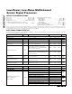
Low-Power, Low-Noise Multichannel Sensor Signal Processor ADDRESS REF ALT NAME FUNCTION 0h R0 P Pointer Register. This register contains the address of the instruction or data in FLASH memory to be fetched. 1h R1 A Accumulator Register. This register generally contains the result of any operation involving two or more registers. It is the accumulator for the multiregister operation result and can be used effectively to carry data from one computation to the next.
MAX1464 Low-Power, Low-Noise Multichannel Sensor Signal Processor Table 2. CPU Ports ADDRESS REF 0h–Ch P0–PC Dh Eh Fh 28 FUNCTION General-Purpose Ports. These ports, P0–PC, can be used to hold intermediate calculation results, often-used calculation coefficients, loop counter values, event counter values, comparison limit values, etc. PD Module Data Port. This port is used to transfer data to and from the various functional modules in the MAX1464.
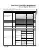
Low-Power, Low-Noise Multichannel Sensor Signal Processor MAX1464 Table 3. Module Registers MODULE NAME REGISTER NAME ADC ADDRESS DESCRIPTION R/W R/ W ADC_Control 00h Initiate conversions and select ADC input. ADC_Data_1 01h Result of ADC conversion on channel 1 input. ADC_Config_1A 02h Settings for channel 1 input and conversion. R/ W ADC_Config_1B 03h Settings for channel 1 input and conversion. R/ W ADC_Data_2 04h Result of ADC conversion on channel 2 input.
MAX1464 Low-Power, Low-Noise Multichannel Sensor Signal Processor Table 5. ADC_Control (Address = 00h) BITS NAME 15–12 — DESCRIPTION 11–8 SE[3:0] 7–3 — 2 CNVT1 1 = Initiate conversion on channel 1 using ADC settings specified in registers ADC_Config_1A and ADC_Config_1B. The ADC result is stored in ADC_Data_1. CPU is halted during the conversion process. This bit is automatically reset to zero when conversion is completed.
Low-Power, Low-Noise Multichannel Sensor Signal Processor MAX1464 Table 7. Single-Ended (SE[3:0]) SE[3:0] PGA RANGE (V/V) ADC +INPUT ADC -INPUT DESCRIPTION 0001 0.99 VBG VSS Bandgap voltage. 0010 0.99 to 244 OUTnSM VSS Output of small op-amp n. 0011 0.99 to 244 OUTnLG VSS Output of large op-amp n. 0100 0.7* VDD** VSS Power-supply voltage. 0101 0.7* VSS VSS Power-supply ground. 0110 0.
MAX1464 Low-Power, Low-Noise Multichannel Sensor Signal Processor Table 11. ADC_Config_2B (Address = 06h) BIT NAME 15–7 — 6–4 BIAS2[2:0] 3–2 — 1–0 REF2[1:0] DESCRIPTION Unused. ADC bias setting to use during conversion of channel 2. BIAS2[2] = MSB. Unused. Reference select for conversion on channel 2. REF2[2] = MSB. Table 12. ADC_Config_TA (Address = 08h) BITS NAME 15–11 PGAT[4:0] Programmable gain to use during conversion of temperature sensor. PGAT[4] = MSB.
Low-Power, Low-Noise Multichannel Sensor Signal Processor RESn[2:0] RESOLUTION (BITS) NO. OF fADC CLOCKS PER CONVERSION 000 9 256 001 10 320 010 12 512 011 13 640 100 14 800 101 15 1280 110 Table 17. ADC Conversion Time (RESn[2:0] and CLKn[2:0], Where n = 1, 2, or T) 16 2048 RESOLUTION (BITS) CONVERSION TIME (ms) 9 CLKn[2:0] = 000 0.256 CLKn[2:0] = 100 4.096 CLKn[2:0] = 111 32.768 10 0.320 5.120 40.960 12 0.512 8.192 65.536 13 0.640 10.240 81.920 14 0.800 12.
MAX1464 Low-Power, Low-Noise Multichannel Sensor Signal Processor Table 19. ADC Bias Current (BIASn[2:0], Where n = 1, 2, or T) BIASn[2:0] FRACTION OF FULL BIAS CURRENT MAXIMUM ADC CLOCK FREQUENCY (Hz) CLKn[2:0] 000 1/8 125k 011 001 2/8 250k 011 010 3/8 250k 010 011 4/8 500k 010 100 5/8 500k 001 101 6/8 500k 001 110 7/8 1M 000 111 8/8 1M 000 Table 20.
Low-Power, Low-Noise Multichannel Sensor Signal Processor SELDAC SELPWM ENDAC ENPWM BUF DAC OFF, PWM OFF, op amp OFF. DOP CONFIGURATION PWRDAC PWROP 0 0 X X 0 0 X DAC OFF, PWM OFF, op amp ON. AMPnP and AMPnM routed to LG op amp. 0 1 0 X 0 0 0 DAC OFF, PWM OFF, op amp ON. LG op amp configured as unity-gain buffer. 0 1 0 X 0 0 1 DAC OFF, PWM OFF, op amp ON. AMPnP and AMPnM routed to SM op amp. 0 1 1 X 0 0 0 DAC OFF, PWM OFF, op amp ON.
MAX1464 Low-Power, Low-Noise Multichannel Sensor Signal Processor Table 22. DOP Module Registers NAME ADDRESS DESCRIPTION POR VALUE DOP1_Data 10h DAC1/PWM1 input data. 0000 DOP1_Control 11h Initiate DAC1 and/or PWM1 conversions. 0000 DOP1_Config 12h DAC1/PWM1 output and DAC 1 reference selection. 0000 DOP2_Data 13h DAC2/PWM2 input data. 0000 DOP2_Control 14h Initiate DAC2 and/or PWM2 conversions. 0000 DOP2_Config 15h DAC2/PWM2 output and DAC 2 reference selection.
Low-Power, Low-Noise Multichannel Sensor Signal Processor MAX1464 Table 26. DOP2_Config (Address = 15h) BIT NAME 15–9 — 8 SELPWM2 7–5 — 4 SELDAC2 3–1 — 0 SELREF2 DESCRIPTION Unused. Select PWM2 output: 1 = OUT2LG, 0 = OUT2SM. Unused. Select DAC2 output: 1 = OUT2LG (large op-amp buffer), 0 = OUT2SM (small op-amp buffer). Unused. Select voltage reference for DAC2: 0 = VDD, 1 = 2 x VREF. Table 27.
MAX1464 Low-Power, Low-Noise Multichannel Sensor Signal Processor Table 28. GPIO1_Control (Address = 40h) BITS NAME 15–6 — DESCRIPTION 5 OUT1 4 EN1 Enable the output driver; 1 = enabled, 0 = disabled, and OUT tri-stated. 3 IN1 When EDGE1 = 0: The value input on GPIO1 is clocked into this bit (Notes 14, 15). When EDGE1 = 1: An edge detection on GPIO1 causes a 1 to be clocked into this bit. 2 CLR1 Clear IN1 bit; 1 = clear IN1 to 0, 0 = IN1 retains its status (Note 16).
Low-Power, Low-Noise Multichannel Sensor Signal Processor MAX1464 Table 32. Timer Prescaler Settings (PS[3:0]) PS[3:1] PS[0] PRESCALER N 000 0 1 001 0 2 010 0 4 011 0 8 100 0 16 101 0 32 110 0 64 111 0 128 000 1 3 001 1 6 010 1 12 011 1 24 100 1 48 101 1 96 110 1 192 111 1 384 Table 33. Power-On Control (Address = 31h) BITS NAME 15–9 — 8 PWRA2D 7–6 — 5 PWRDAC2 DESCRIPTION Unused. Power for ADC: 1 = power enabled, 0 = disabled. Unused.
MAX1464 Low-Power, Low-Noise Multichannel Sensor Signal Processor Table 34. Oscillator Control (Address = 32h) BITS 15–13 12–8 NAME — OSC[4:0] DESCRIPTION Unused. Oscillator trim setting. OSC[4] = MSB. 7–6 — Unused. 5–4 — Reserved 0. 3–1 — Unused. 0 ENCKOUT Enable clock output: 1 = enable internal clock output on CKIO based on CKSEL inputs, 0 = disable. Table 35.
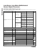
Low-Power, Low-Noise Multichannel Sensor Signal Processor Bit 15 Bit 14 Bit 13 Bit 12 Bit 11 Bit 10 Bit 9 Bit 8 Bit 7 Bit 6 Bit 5 Bit 4 Register 00h ADC_Control X X X X SE[3] SE[2] SE[1] SE[0] X X X X Register 01h ADC_Data_1 (for Channel Input 1, Uncompensated, and Read-Only Register) Bit 3 Bit 2 X CNVT1 Bit 1 Bit 0 CNVT2 CNVTT LSB MSB Register 02h ADC_Config_1A (for Channel 1) X RES1[2] RES1[1] RES1[0] CO1[3] CO1[2] CO1[1] CO1[0] Register 03h ADC_Config_1B (for Channel 1) X X X X X X X X X BIAS1[
MAX1464 Low-Power, Low-Noise Multichannel Sensor Signal Processor Table 38. Internal Register Set Address (IRSA) Decoding IRSA[3:0] REGISTER NIBBLE ADDRESSED 0000 DHR[3:0] Write IRSD[3:0] to DHR[3:0]. 0001 DHR[7:4] Write IRSD[3:0] to DHR[7:4]. 0010 DHR[11:8] Write IRSD[3:0] to DHR[11:8]. 0011 DHR[15:12] Write IRSD[3:0] to DHR[15:12]. 0100 PFAR[3:0] Write IRSD[3:0] to PFAR[3:0]. 0101 PFAR[7:4] Write IRSD[3:0] to PFAR[7:4]. 0110 PFAR[11:8] Write IRSD[3:0] to PFAR[11:8].
Low-Power, Low-Noise Multichannel Sensor Signal Processor MAX1464 Table 40. Interface Mode Register (IMR) Decoding IRSD DESCRIPTION 0000 Place the MAX1464 into a 4-wire serial interface (DI cannot be connected to DO). 0001 Place the MAX1464 into a 3-wire serial interface (DI can be externally connected to DO). 0010–1111 Unused. Table 41. Instruction Set TWO’S COMP NO. OF REGISTERS INVOLVED NO. OF CYCLES NO. OF BYTES Load register X from program memory. Y 1 3 3 Clear X-reg.
Low-Power, Low-Noise Multichannel Sensor Signal Processor CS DO DI SCLK MAX1464 Functional Diagram SERIAL INTERFACE VDD INP1 CO DAC INM1 4kB FLASH MEMORY 16-BIT CPU POWERON RESET VDDF VSS VSSF INP2 Σ MUX PGA ADC CKIO INM2 CKSEL DIGITAL I/O TEMP SENSOR GPIO2 DAC 1 PWM 1 DAC 2 PWM 2 GPIO1 EXTERNAL REFERENCE INPUT BANDGAP REFERENCE OUT2SM SM AMP2M OUT2LG LG AMP2P OUT1SM SM AMP1M OUT1LG AMP1P LG VREF Chip Information TRANSISTOR COUNT: 70,921 (not including FLASH) PROCES
INM2 INP2 INM1 INP1 TEMPERATURE SENSOR VSS M U X REF VBG OUTnSM OUTnLG VDD VSS DACnOUT VIA OUTnSM DACnOUT VIA OUTnLG INPn INMn 2 3 4 5 6 7 8 9 SINGLE-ENDED 1 NO.
OUT2LG AMP2P AMP2M OUT2SM OUT1LG AMP1P AMP1M OUT1SM SW11 SW10 SW11 SW10 SW5 SW0 SW5 SW0 LG2 SM2 LG1 SM1 SW6 SW1 SW6 SW1 SW7 SW2 SW7 SW2 SW9 SW8 SW4 SW3 SW9 SW8 SW4 SW3 REF PWM2 DAC2 REF PWM1 DAC1 DOP2 MODULE OpAmp_Config DOP2_Config 15h 30h DOP2_Control DOP2_Data DOP1 MODULE OpAmp_Config 14h 13h 2 x VREF VDD 30h DOP1_Config 12h DOP1_Data DOP1_Control 11h 10h 2 x VREF VDD TMR_Config TMR_Control GPION_Control GPION_Control 21h 20h TRI-STA
Low-Power, Low-Noise Multichannel Sensor Signal Processor SSOP EPS 2 1 INCHES E H MILLIMETERS DIM MIN MAX MIN MAX A 0.068 0.078 1.73 1.99 A1 0.002 0.008 0.05 0.21 B 0.010 0.015 0.25 0.38 C D 0.20 0.09 0.004 0.008 SEE VARIATIONS E 0.205 e 0.212 0.0256 BSC 5.20 INCHES D D D D D 5.38 MILLIMETERS MIN MAX MIN MAX 0.239 0.239 0.278 0.249 0.249 0.289 6.07 6.07 7.07 6.33 6.33 7.33 0.317 0.397 0.328 0.407 8.07 10.07 8.33 10.33 N 14L 16L 20L 24L 28L 0.65 BSC H 0.