
Instruction Manual

2 ______________________________________________________________________________________
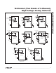
MAX14805/MAX14806
16-Channel (Two Banks of 8-Channel),
High-Voltage Analog Switches
Stresses beyond those listed under “Absolute Maximum Ratings” may cause permanent damage to the device. These are stress ratings only, and functional
operation of the device at these or any other conditions beyond those indicated in the operational sections of the specifications is not implied. Exposure to absolute
maximum rating conditions for extended periods may affect device reliability.
(All voltages referenced to GND.)
V
DD
Logic Supply Voltage ......................................-0.3V to +7V
V
PP
- V
NN
Supply Voltage ..................................................230V
V
PP
Positive Supply Voltage ..............................-0.3V to +220V
V
NN
Negative Supply Voltage ............................+0.3V to -220V
Logic Inputs Voltage (LE, DIN1, DIN2) ..................-0.3V to +7V
Analog Signal Range (SW_) .......(-0.3V + V
NN
) to (V
NN
+ 200V)
Peak Analog Signal Current per Channel ..............................3A
Continuous Power Dissipation (T
A
= +70NC)
48-Pin TQFP (derate 22.7mW/NC above +70NC) ......1818mW
Junction-to-Ambient Thermal Resistance
B
JA
(Note 1) .................................................................44NC/W
Junction-to-Ambient Thermal Resistance
B
JC
(Note 1) ................................................................10NC/W
Operating Temperature Range .......................... -40NC to +85NC
Storage Temperature Range ............................ -65NC to +150NC
Junction Temperature ................................................... +150NC
Lead Temperature (soldering, 10s) ................................+300NC
Soldering Temperature (reflow) ......................................+260NC
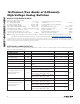
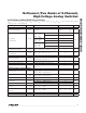
ELECTRICAL CHARACTERISTICS
(V
DD
= +2.7V to +5.5V, V
PP
= +40V to (V
NN
+ 200V), V
NN
= -40V to -160V, T
A
= T
MIN
to T
MAX
, unless otherwise noted. Typical
values are at T
A
= +25NC.) (Note 2)
ABSOLUTE MAXIMUM RATINGS
Note 1. Package thermal resistances were obtained using the method described in JEDEC specification JESD51-7, using a four-
layer board. For detailed information on package thermal considerations, refer to www.maxim-ic.com/thermal-tutorial.
PARAMETER SYMBOL CONDITIONS MIN TYP MAX UNITS
POWER SUPPLIES
V
DD
Supply Voltage V
DD
2.7 5.5 V
V
PP
Supply Voltage V
PP
40 100
V
NN
+ 220
V
V
NN
Supply Voltage V
NN
-160 -100 -15 V
V
DD
Supply Quiescent Current I
DDQ
5
FA
V
DD
Supply Dynamic Current I
DDD
V
DD
= +5V, LE = GND, f
DIN1
= f
DIN2
=
5MHz
2 mA
V
PP
Supply Quiescent Current I
PPQ
10
FA
V
PP
Supply Dynamic Current
(All Channel Switching
Simultaneously)
I
PP
V
PP
= +40V, V
NN
= -160V, f
SW_
= 50kHz,
f
DIN1
= f
DIN2
= 50kHz, LE = GND
5
mA
V
PP
= +100V, V
NN
= -100V, f
SW_
= 50kHz,
f
DIN1
= f
DIN2
= 50kHz, LE = GND
6
V
PP
= +160V, V
NN
= -40V, f
SW_
= 50kHz,
f
DIN1
= f
DIN2
= 50kHz, LE = GND
7
V
NN
Supply Quiescent Current I
NNQ
10
FA
V
NN
Supply Dynamic Current
(All Channel Switching
Simultaneously)
I
NN
V
PP
= +40V, V
NN
= -160V, f
SW_
= 50kHz,
f
DIN1
= f
DIN2
= 50kHz, LE = GND
5.5
mA
V
PP
= +100V, V
NN
= -100V, f
SW_
= 50kHz,
f
DIN1
= f
DIN2
= 50kHz, LE = GND
5
V
PP
= +160V, V
NN
= -40V, f
SW_
= 50kHz,
f
DIN1
= f
DIN2
= 50kHz, LE = GND
4.5