
User guide
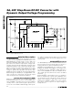


MAX15020
2A, 40V Step-Down DC-DC Converter with
Dynamic Output-Voltage Programming
14 ______________________________________________________________________________________
Compensation Design
The MAX15020 uses a voltage-mode control scheme
that regulates the output voltage by comparing the
error-amplifier output (COMP) with an internal ramp to
produce the required duty cycle. The output lowpass
LC filter creates a double pole at the resonant frequen-
cy, which has a gain drop of -40dB/decade. The error
amplifier must compensate for this gain drop and
phase shift to achieve a stable closed-loop system.
The basic regulator loop consists of a power modulator,
an output feedback divider, and a voltage error amplifi-
er. The power modulator has a DC gain set by V
IN
/
V
RAMP
, with a double pole and a single zero set by the
output inductance (L), the output capacitance (C
OUT
)
(C6 in the Figure 2) and its ESR. The power modulator
incorporates a voltage feed-forward feature, which auto-
matically adjusts for variations in the input voltage
resulting in a DC gain of 9. The following equations
define the power modulator:
The switching frequency is internally set at 300kHz or
500kHz, or can vary from 100kHz to 500kHz when driven
with an external SYNC signal. The crossover frequency
(f
C
), which is the frequency when the closed-loop gain is
equal to unity, should be set as f
SW
/ 2π or lower.
The error amplifier must provide a gain and phase
bump to compensate for the rapid gain and phase loss
from the LC double pole. This is accomplished by utiliz-
ing a Type 3 compensator that introduces two zeros
and three poles into the control loop. The error amplifier
has a low-frequency pole (f
P1
) near the origin.
In reference to Figures 3 and 4, the two zeros are at:
And the higher frequency poles are at:
Compensation when f
C
< f
ESR
Figure 3 shows the error-amplifier feedback as well as
its gain response for circuits that use low-ESR output
capacitors (ceramic). In this case f
ZESR
occurs after f
C
.
f
Z1
is set to 0.8 x f
LC(MOD)
and f
Z2
is set to f
LC
to com-
pensate for the gain and phase loss due to the double
pole. Choose the inductor (L) and output capacitor
(C
OUT
) as described in the
Inductor Selection
and
Output Capacitor Selection
sections.
Choose a value for the feedback resistor R6 in Figure 3
(values between 1kΩ and 10kΩ are adequate).
C12 is then calculated as:
f
C
occurs between f
Z2
and f
P2
. The error-amplifier gain
(GEA) at f
C
is due primarily to C11 and R9.
Therefore, GEA(f
C
) = 2π x f
C
x C11 x R9 and the modu-
lator gain at f
C
is:
Since G
EA(fC)
x G
MOD(fC)
= 1, C11 is calculated by:
f
P2
is set at 1/2 the switching frequency (f
SW
). R6 is
then calculated by:
Since R7 >> R6, R7 + R6 can be approximated as R7.
R7 is then calculated as:
f
P3
is set at 5 x f
C
. Therefore, C13 is calculated as:
C
C
CRf
P
13
12
2129 1
3
=
×××
−π
R
fC
LC
7
1
211
=
××π
R
Cf
SW
6
1
21105
=
×××π .
C
fLC
RG
C OUT
MOD DC
11
2
9
=
×× ×
×
π
()
G
G
LC f
MOD fC
MOD DC
OUT C
()
()
()
=
×× ×2
2
2
π
C
fR
LC
12
1
208 9
=
×××π .
f
RC
and f
R
CC
CC
PP23
1
2611
1
29
12 13
12 13
=
××
=
××
×
+
⎛
⎝
⎜
⎞
⎠
⎟
π
π
f
RC
and f
RR C
ZZ12
1
2912
1
26711
=
××
=
×+×ππ
()
G
V
V
f
LC
f
C ESR
MOD DC
IN
RAMP
LC
ESR
OUT
()
==
=
×
=
××
9
1
2
1
2
π
π