
Manual

MAX1507
Layout and Bypassing
Connect a 1µF ceramic input capacitor as close to the
device as possible. Provide a large copper GND plane
to allow the exposed paddle to sink heat away from the
device. Connect the battery to BATT as close to the
device as possible to provide accurate battery voltage
sensing. Make all high-current traces short and wide to
minimize voltage drops. For an example layout, refer to
the MAX1507/MAX1508 evaluation kit layout.
Chip Information
TRANSISTOR COUNT: 1812
PROCESS: BiCMOS
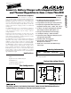
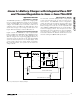
Linear Li+ Battery Charger with Integrated Pass FET
and Thermal Regulation in 3mm x 3mm Thin DFN
10 ______________________________________________________________________________________
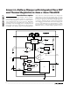
MAX1507
1µF
15.4kΩ
4.3kΩ
IN
CHG
1µF
4.2V Li+
BATT
EN
N
GND
SYSTEM
TEMP
VL
ISET
USB PORT
VBUS
GND
D+
D-
VI/O
ROHM
DTC114EM
VI/O
HIGH: 435mA, LOW: 95mA
0.47µF
Figure 4. USB Battery Charger