
Manual

MAX1507
Linear Li+ Battery Charger with Integrated Pass FET
and Thermal Regulation in 3mm x 3mm Thin DFN
_______________________________________________________________________________________ 5
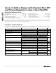
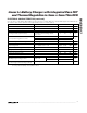
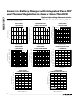
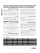
Typical Operating Characteristics (continued)
(V
IN
= 5V, V
BATT
= 4.0V, TEMP = EN = CHG = unconnected, R
ISET
= 2.8kΩ to GND, C
IN
= 1µF, C
BATT
= 1µF, C
VL
= 0.47µF, T
A
=
+25°C, unless otherwise noted.)
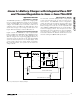
0
200
600
400
800
100
300
700
500
900
1000
-40 10-15 35 60 85
CHARGE CURRENT
vs. AMBIENT TEMPERATURE (TEMP = OPEN)
MAX1507 toc09
AMBIENT TEMPERATURE (
°
C)
CHARGE CURRENT (mA)
V
BATT
= 4.0V
V
BATT
= 3.6V
R
ISET
= 1.87k
Ω
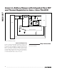
0
200
600
400
800
100
300
700
500
900
1000
-40 10-15 35 60 85
CHARGE CURRENT
vs. AMBIENT TEMPERATURE (TEMP = GND)
MAX1507 toc10
AMBIENT TEMPERATURE (
°
C)
CHARGE CURRENT (mA)
V
BATT
= 4.0V
V
BATT
= 3.6V
R
ISET
= 1.87k
Ω
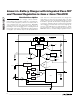
Pin Description
PIN
NAME
FUNCTION
1 VL Internally Generated Logic Supply for Chip. Bypass VL to GND with a 0.47µF capacitor.
2 IN Input Supply Voltage. Bypass IN to GND with a 1µF capacitor to improve line noise and transient rejection.
3 GND Ground. Connect GND and exposed pad to a large copper trace for maximum power dissipation.
4 ISET
Charge-Current Program and Fast-Charge Current Monitor. Output current from ISET is 0.958mA per amp of
battery charging current. The charging current is set by connecting a resistor from ISET to GND. Fast-charge
current = 1461V / R
ISET
Ω.
5 EN
Logic-Level Enable Input. Drive EN high to disable charger. Pull EN low or float for normal operation. EN has
an internal 200kΩ pulldown resistor.
6 TEMP
Three-Level Input Pin. Connect TEMP to VL, GND, or leave floating. Sets maximum die temperature for
thermal regulation loop. Connection to GND = +90°C, floating = +100°C, VL = +130°C. TEMP is Hi-Z during
shutdown.
7 BATT Li+ Battery Connection. Bypass BATT to GND with a capacitor of at least 1µF per ampere of charge current.
8 CHG
Charging Indicator, Open-Drain Output. CHG goes low (and can turn on an LED) when charging begins.
CHG is high impedance when the battery current drops below 10% of the fast-charging current, or when EN
is high. Connect a pullup resistor to the µP’s I/O voltage when interfacing with a µP logic input.
— PAD
Exposed Pad. Connect exposed pad to a large copper trace for maximum power dissipation. The pad is
internally connected to GND.