
Manual
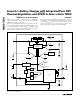

MAX1508
Linear Li+ Battery Charger with Integrated Pass FET,
Thermal Regulation, and
ACOK
in 3mm x 3mm TDFN
2 _______________________________________________________________________________________
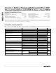
ABSOLUTE MAXIMUM RATINGS
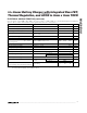
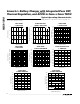
ELECTRICAL CHARACTERISTICS
(V
IN
= 5V, V
BATT
= 4.0V, ACOK = EN = CHG = unconnected, R
ISET
= 2.8kΩ to GND, C
VL
= 0.47µF, BATT bypassed to GND with
1µF, T
A
= -40°C to +85°C, unless otherwise noted. Typical values are at T
A
= +25°C.) (Note 1)
Stresses beyond those listed under “Absolute Maximum Ratings” may cause permanent damage to the device. These are stress ratings only, and functional
operation of the device at these or any other conditions beyond those indicated in the operational sections of the specifications is not implied. Exposure to
absolute maximum rating conditions for extended periods may affect device reliability.
IN, CHG to GND .....................................................-0.3V to +14V
VL, BATT, ISET, EN, ACOK to GND .........................-0.3V to +6V
VL to IN...................................................................-14V to +0.3V
IN to BATT Continuous Current.............................................0.9A
Continuous Power Dissipation (T
A
= +70°C)
8-Pin TDFN (derate 24.4mW/°C above +70°C) .........1951mW
Short-Circuit Duration.................................................Continuous
Operating Temperature Range ...........................-40°C to +85°C
Junction Temperature......................................................+150°C
Storage Temperature Range .............................-65°C to +150°C
Lead Temperature (soldering, 10s) .................................+300°C
PARAMETER CONDITIONS MIN TYP MAX UNITS
Input Voltage Range 013V
Input Operating Range 4.25 6.50 V
V
IN
- V
BATT
, V
IN
rising 20 40 60
ACOK Trip Point, IN
V
IN
- V
BATT
, V
IN
falling 15 30 45
mV
V
IN
rising 6.5 7 7.5
Overvoltage Lockout Trip Point
V
IN
hysteresis 0.11
V
Charging (I
IN
- I
BATT
)12
Disabled, EN = VL 0.8 1.5IN Input Current
OFF state (V
IN
= V
BATT
= 4.0V) 0.065
mA
VL Output Voltage I
VL
= 100µA 3.3 V
VL Load Regulation I
VL
= 100µA to 2mA -71 -200 mV
VL Temperature Coefficient I
VL
= 100µA -2 mV/°C
V
IN
rising 2.95
VL Undervoltage Lockout Trip Point
Hysteresis 0.17
V
V
IN
= 0 to 4V 3 10
BATT Input Current
EN = VL 4 10
µA
Maximum RMS Charge Current 0.8 A
T
A
= 0°C to +85°C 4.162 4.2 4.238
Battery Regulation Voltage I
BATT
= 0
T
A
= -40°C to +85°C 4.150 4.2 4.250
V
BATT Removal Detection Threshold V
BATT
rising 4.4 4.67 4.9 V