
Owner manual
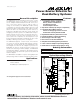


MAX1538
Power-Source Selector for
Dual-Battery Systems
_______________________________________________________________________________________ 5
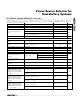
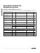
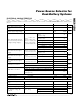
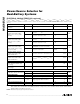
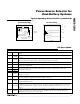
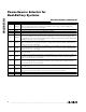
ELECTRICAL CHARACTERISTICS
(V
BATA
= V
BATB
= V
CHGIN
= 16.8V, C
VDD
= 1µF, V
MINVA
= V
MINVB
= 0.93V, V
EXTLD
= V
ADPIN
= 28V, V
CHRG
= V
BATSEL
= V
RELRN
= 0,
C
ADPPWR
= C
REVBLK
= C
ADPBLK
= C
DISBAT
= C
DISA
= C
DISB
= C
CHGA
= C
CHGB
= 4.7nF, T
A
= -40°C to +85°C, unless otherwise noted.)
(Note 2)
PARAMETER CONDITIONS
MIN MAX
UNITS
ADPIN, EXTLD Supply Voltage
Range
4.75 28.00
V
CHGIN, BATA, BATB, and
BATSUP Supply Voltage Range
4.75 19.00
V
V
ADPIN
= highest,
V
ADPPWR
= high
50
V
ADPIN
= highest,
V
ADPPWR
= low
54
V
BATA
= highest, V
DISA
= high
42
V
BATA
= highest, V
DISA
= low
50
V
BATB
= highest, V
DISB
= high
42
V
BATB
= highest, V
DISB
= low
50
ADPIN, BATA, BATB, BATSUP
Quiescent Current (Current from
the Highest Voltage Supply)
V
B AT A
= 4.75V to 19V ,
V
B AT B
= 4.75V to 19V ,
V
B AT S U P
= 4.75V to 19V ,
V
A D P IN
= 4.75V to 28V ,
no exter nal l oad at V
D D
V
BATSUP
= highest 40
µA
V
ADPPWR
= high 1
ADPIN Quiescent Current (ADPIN
Current When Not the Highest
Voltage)
V
ADPIN
= 4.75V to 18V,
no external load at V
DD
V
ADPPWR
= low 9
µA
V
DISA
= high 7.5
BATA Quiescent Current (BATA
Current When Not the Highest
Voltage)
V
BATA
= 4.75V to 19V,
no external load at V
DD
V
DISA
= low 16
µA
V
DISB
= high 7.5
BATB Quiescent Current (BATB
Current When Not the Highest
Voltage)
V
BATB
= 4.75V to 19V,
no external load at V
DD
V
DISB
= low 16
µA
Adapter selected (REVBLK or ADPBLK pins low) 9.5
EXTLD Quiescent Current
Adapter not selected (REVBLK and ADPBLK pins high) 1.0
µA
AC or ai r l i ne state ( C H G A, C H GB, and D IS BAT p i ns hi g h) 1.5
Charge state (CHGA or CHGB pin low, DISBAT pin high)
10
CHGIN Quiescent Current
Discharge or relearn state (CHGA or CHGB pin low,
DISBAT pin low)
18.5
µA
LINEAR REGULATOR
V
DD
Output Voltage I
VDD
= 0 to 100µA
3.270 3.330
V
V
DD
Undervoltage Lockout Rising edge, relative to regulation point -60 -10 mV
COMPARATORS
ACDET, AIRDET Input Voltage
Range
0 5.5 V
ACDET, AIRDET Trip Threshold Input falling
1.94 2.06
V
MINV_ Operating Voltage Range
0.93 2.60
V
V
MINV_
= 0.93V
4.59 4.72
V
MINV_
= 1.5V 7.4 7.6
BAT_ Minimum Voltage Trip
Threshold
V
BAT_
falling
V
MINV_
= 2.6V
12.86 13.14
V