
User Manual


MAX1578/MAX1579
Complete Bias and White LED Power Supplies
for Small TFT Displays
6 _______________________________________________________________________________________
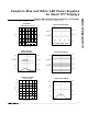
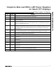
-5.0
-3.5
-4.0
-4.5
-3.0
-2.5
-2.0
-1.5
-1.0
POS
NEG
-0.5
0
04020 60 80 100
POS AND NEG LOAD REGULATION
MAX1578toc12
LOAD CURRENT (
µ
A)
VOLTAGE DROOP (%)
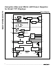
-0.6
-0.4
-0.5
-0.2
-0.3
-0.1
0
025
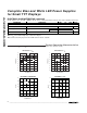
MAIN OUTPUT LOAD REGULATION
MAX1578toc11
LOAD CURRENT (mA)
VOLTAGE DROOP (%)
1051520
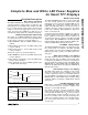
PIN NAME FUNCTION
1 MAIN
LDO Output and the POS and NEG Charge-Pump Inputs. V
MAIN
is regulated to 5V. Bypass to GND
with a 1µF capacitor. Output is internally discharged with a 1kΩ resistor when V
ONBIAS
= 0V.
2 CU1 POS Charge-Pump Capacitor Connection 1. Connect a 1µF capacitor between CU1 and PMP.
3 CU2 POS Charge-Pump Capacitor Connection 2. Connect a 1µF capacitor between CU2 and PMPB.
4 CU3 POS Charge-Pump Capacitor Connection 3. Connect a 1µF capacitor between CU3 and GND.
5 POS
Output of Positive (3x) Charge Pump. Bypass POS to GND with a 1µF capacitor. POS is internally
discharged with a 3kΩ resistor when V
ONBIAS
= 0V.
6PMP
Charge-Pump Capacitor Connection. Connect a 1µF capacitor between PMP and CU1 and another
1µF capacitor between PMP and CD1.
7 PMPB
Charge-Pump Capacitor Connection. Connect a 1µF capacitor between PMPB and CU2 and another
1µF capacitor between PMPB and CD2. PMPB is 180° out of phase with PMP.
8 CD1
NEG Charge-Pump Capacitor Connection 1. Connect a 1µF capacitor and a 200Ω ±5% resistor in
series between CD1 and PMP.
9 CD2
NEG Charge-Pump Capacitor Connection 2. Connect a 1µF capacitor and a 200Ω ±5% resistor in
series between CD2 and PMPB.
10 NEG
Output of Inverting (-2x) Charge Pump. Bypass NEG to GND with a 1µF capacitor. Output is internally
discharged with a 1.5kΩ resistor when V
ONBIAS
= 0V.
Pin Description
Typical Operating Characteristics (continued)
(Circuit of Figure 3, V
IN
= 3.6V, I
LED
= 20mA, 4 LEDs, CTRL = IN, T
A
= +25°C, unless otherwise noted.)