
User Manual


MAX1578/MAX1579
Complete Bias and White LED Power Supplies
for Small TFT Displays
_______________________________________________________________________________________ 7
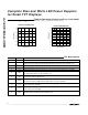
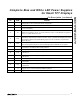
PIN NAME FUNCTION
11 ONBIAS
Logic Input to Enable V
DD
, MAIN, POS, and NEG Charge Pumps. Drive ONBIAS high to enable all the
charge pumps. Connect to GND to disable the charge pumps.
12 GND Ground. Connect to PGND and the exposed pad directly under the IC.
13 COMP
LED Driver Compensation. Connect a 0.1µF from COMP to GND. C
COMP
stabilizes the driver and
sets the soft-start time.
14 CS
Current-Sense Feedback Input. Connect a resistor from CS to GND to set the LED current. For the
MAX1578, CS regulates to V
CTRL
/ 5 or 0.327V, whichever is lower. For the MAX1579, CS regulates to
V
CTRL
/ 5 or 0.340V, whichever is lower.
15 CTRL
LE D Br i g htness C ontr ol Inp ut. C onnect C TRL to a 0.24V to 1.65V i np ut to set the b r i g htness of the
exter nal LE D s. H ol d C TRL b el ow 100m V for m or e than 10.5m s, to shut d ow n the LE D d r i ver . D r i ve C TRL
w i th a 200H z to 200kH z unfi l ter ed P W M d i m m i ng si g nal for D C LE D cur r ent that i s p r op or ti onal to the
si g nal ’ s d uty cycl e.
16 OUT
Over vol tag e S ense Inp ut. The M AX 1578/M AX 1579 tur n off the n- channel M OS FE T w hen V
OU T
exceed s 34V .
Once V
OU T
d r op s b el ow 32V , the IC r e- enter s soft- star t. Byp ass OU T to GN D w i th a 0.1µF cap aci tor .
17 LX
Inductor Connection. Connect to the switched side of the external inductor as well as the anode of the
external diode. LX is high impedance during shutdown.
18 PGND Power Ground. Connect to GND and the exposed pad directly under the IC.
19 C1N
Main Charge-Pump Transfer Capacitor Negative Connection 1. Connect a 2.2µF capacitor between
C1N and C1P.
20 C2N
Main Charge-Pump Transfer Capacitor Negative Connection 2. Connect a 2.2µF capacitor between
C2N and C2P.
21 IN P ow er - S up p l y Inp ut. C onnect to a 2.7V to 5.5V i np ut sup p l y. Byp ass IN to GN D w i th a 4.7µF cap aci tor .
22 C2P
Main Charge-Pump Transfer Capacitor Positive Connection 2. Connect a 2.2µF capacitor between
C2P and C2N.
23 C1P
Main Charge-Pump Transfer Capacitor Positive Connection 1. Connect a 2.2µF capacitor between
C1P and C1N.
24 V
DD
Regulated Main Charge-Pump Output. V
DD
is regulated to 5.5V. Bypass V
DD
to GND with a 4.7µF
capacitor. V
DD
is connected to IN when ONBIAS is pulled low.
— EP Exposed Paddle. Connect directly to a ground plane, GND, and PGND directly under the IC.
Pin Description (continued)