9-5040; Rev 0; 10/09 6-Channel, Flash-Configurable System Manager with Nonvolatile Fault Registers The MAX16068 flash-configurable system manager monitors and manages up to six system voltages simultaneously. The MAX16068 integrates an analogto-digital converter (ADC). Device configuration information, including overvoltage and undervoltage limits, time delay settings is stored in nonvolatile flash memory.
MAX16068 6-Channel, Flash-Configurable System Manager with Nonvolatile Fault Registers ABSOLUTE MAXIMUM RATINGS VCC to GND................……………………………….-0.3V to +15V MON_, SCL, SDA, A0 to GND.................................-0.3V to +6V EN, TCK, TMS, TDI to GND.....................................-0.3V to +4V TDO to GND.............................................-0.3V to (VDBP + 0.3V) RESET, GPIO_ (configured as open-drain) to GND......................-0.
6-Channel, Flash-Configurable System Manager with Nonvolatile Fault Registers (VCC = 2.8V to 14V, TA = TJ = -40NC to +85NC, unless otherwise specified. Typical values are at VABP = VDBP = VCC = 3.3V, TA = +25NC.
MAX16068 6-Channel, Flash-Configurable System Manager with Nonvolatile Fault Registers ELECTRICAL CHARACTERISTICS (continued) (VCC = 2.8V to 14V, TA = TJ = -40NC to +85NC, unless otherwise specified. Typical values are at VABP = VDBP = VCC = 3.3V, TA = +25NC.) (Note 2) PARAMETER SYMBOL CONDITIONS MIN TYP MAX UNITS 400 kHz SMBus TIMING Serial Clock Frequency fSCL Bus Free Time Between STOP and START Condition tBUF 1.3 Fs START Condition Setup Time tSU:STA 0.
6-Channel, Flash-Configurable System Manager with Nonvolatile Fault Registers MAX16068 SDA tBUF tSU:DAT tSU:STA tHD:DAT tLOW tHD:STA tSU:STO SCL tHIGH tHD:STA tR tF START CONDITION STOP CONDITION REPEATED START CONDITION START CONDITION Figure 1. SMBus Timing Diagram t1 t2 t3 TCK t4 t5 TDI, TMS t6 t7 TDO Figure 2.
Typical Operating Characteristics (Typical values are at VCC = 3.3V, TA = +25NC.) NORMALIZED MON_THRESHOLD vs. TEMPERATURE VCC SUPPLY CURRENT vs. VCC SUPPLY VOLTAGE TA = +85°C 2.5 2.0 TA = +25°C TA = -40°C 1.5 ABP AND DBP REGULATORS ACTIVE 1.0 0.5 1.040 1.025 1.010 0.995 0.980 5.6V RANGE HALF-SCALE PUV THRESHOLD 0.965 0.950 0 0 2 4 6 8 VCC (V) 10 12 -40 14 0 20 40 60 80 TEMPERATURE (°C) NORMALIZED EN THRESHOLD vs. TEMPERATURE TRANSIENT DURATION vs. THRESHOLD OVERDRIVE (EN) 1.025 1.
6-Channel, Flash-Configurable System Manager with Nonvolatile Fault Registers OUTPUT VOLTAGE vs. SINK CURRENT (OUT = LOW) MR TO RESET PROPAGATION DELAY vs. TEMPERATURE MAX 900 0.40 0.35 0.30 VOUT (V) 600 500 MIN 0.25 0.20 0.15 400 RESET, GPIO_ 0.10 300 0.05 200 0 100 -40 -20 0 20 40 60 5 0 80 10 OUTPUT-VOLTAGE HIGH vs. SOURCE CURRENT (PUSH-PULL OUTPUT) INTEGRAL NONLINEARITY vs. CODE RESET 0.8 0.6 3.1 0.4 GPIO_ 3.0 INL (LSB) VOUT (V) MAX16068 toc10 3.3 2.9 2.8 0.2 0 -0.
6-Channel, Flash-Configurable System Manager with Nonvolatile Fault Registers MON1 GND ABP VCC DBP EN TOP VIEW MON2 21 20 19 18 17 16 15 MON3 22 14 N.C. MON4 23 13 N.C. MON5 24 12 TMS MON6 25 11 TCK MAX16068 RESET 26 10 TDI GPIO1 27 9 TDO 8 SDA GPIO4 4 5 GND GPIO3 3 GPIO6 2 GPIO5 1 6 7 AO EP* + GPIO2 28 SCL MAX16068 Pin Configuration THIN QFN (5mm x 5mm) *CONNECT EXPOSED PAD TO GND.
6-Channel, Flash-Configurable System Manager with Nonvolatile Fault Registers PIN NAME FUNCTION 16 DBP Digital Bypass. All push-pull outputs are referenced to DBP. Bypass DBP with a 1FF capacitor to GND. 17 VCC Power-Supply Input. Bypass VCC to GND with a 10FF ceramic capacitor. 18 ABP Analog Bypass. Bypass ABP to GND with a 1FF ceramic capacitor. 20–25 MON1– MON6 Monitor Voltage Inputs. Set the monitor voltage range through the configuration registers.
MAX16068 6-Channel, Flash-Configurable System Manager with Nonvolatile Fault Registers Detailed Description The MAX16068 monitors up to six system power supplies. The monitoring phase begins after boot-up if EN is high and the software enable bit is set to ‘1’. An internal multiplexer cycles through each MON_ input. At each multiplexer stop, the 10-bit ADC converts the monitored analog voltage to a digital result and stores the result in a register.
6-Channel, Flash-Configurable System Manager with Nonvolatile Fault Registers MON_ configuration registers are set to ’11,’ MON_ voltages are not monitored and the multiplexer does not stop at these inputs, decreasing the total cycle time. These inputs cannot be configured to trigger fault conditions. Set r73h[2] to ‘1’ to enable monitoring functionality. Faults are not recorded when the device is in margining mode. Set r73h[2] to ‘0’ for normal functionality.
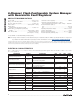
MAX16068 6-Channel, Flash-Configurable System Manager with Nonvolatile Fault Registers Table 3. ADC Configuration Registers REGISTER ADDRESS FLASH ADDRESS 43h BIT RANGE [1:0] [3:2] MON2 Full-Scale Range 00 = 5.6V 01 = 2.8V 10 = 1.4V 11 = channel not converted [5:4] MON3 Full-Scale Range 00 = 5.6V 01 = 2.8V 10 = 1.4V 11 = channel not converted [7:6] MON4 Full-Scale Range 00 = 5.6V 01 = 2.8V 10 = 1.4V 11 = channel not converted [1:0] MON5 Full-Scale Range 00 = 5.6V 01 = 2.8V 10 = 1.
6-Channel, Flash-Configurable System Manager with Nonvolatile Fault Registers When GPIO1–GPIO6 are configured as general-purpose inputs/outputs, read values from the GPIO_ ports through r1Eh and write values to GPIO_s through r3Eh. Note that r3Eh has a corresponding flash register, which programs the default state of a general-purpose output. See Table 7 for more information on reading and writing to the GPIO_. Table 5.
MAX16068 6-Channel, Flash-Configurable System Manager with Nonvolatile Fault Registers ALERT GPIO1 is configurable as the SMBus alert signal, ALERT. ALERT asserts when any fault condition occurs. When the SMBus host sends the ARA (Alert Response Address), the MAX16068 responds with its slave address and deasserts ALERT. ALERT is an open-drain output. Set the ARAEN bit in r40h[4] to ‘1’ to disable the ARA feature. Under these conditions, the device does not respond to an ARA on the SMBus line.
6-Channel, Flash-Configurable System Manager with Nonvolatile Fault Registers The MAX16068 is capable of measuring overvoltage and undervoltage fault events. Fault conditions are detected at the end of each ADC conversion. An overvoltage event occurs when the voltage at a monitored input exceeds the overvoltage threshold for that input. An undervoltage event occurs when the voltage at a monitored input falls below the undervoltage threshold.
MAX16068 6-Channel, Flash-Configurable System Manager with Nonvolatile Fault Registers Deglitch Fault conditions are detected at the end of each conversion. When the voltage on an input falls outside a monitored threshold for one acquisition, the input multiplexer remains on that channel and performs several successive conversions. To trigger a fault, the input must stay outside the threshold for a certain number of acquisitions as determined by the deglitch setting in r74h[6:5] (see Table 10).
6-Channel, Flash-Configurable System Manager with Nonvolatile Fault Registers The SMB Alert (ALERT) bit is set if the MAX16068 has asserted the SMBus Alert output. Clear by writing a ‘1’. See the SMBALERT (ALERT) section for more details. Critical Faults During normal operation, a fault condition can be stored in the flash memory by setting the appropriate critical fault enable bits.
MAX16068 6-Channel, Flash-Configurable System Manager with Nonvolatile Fault Registers Logged fault information is stored in flash registers r200h–r208h (see Table 13). After fault information is logged, the flash is locked and must be unlocked to enable a new fault log to be stored. Write a ‘0’ to r8Ch[1] to unlock the configuration flash. Fault information can be configured to store ADC conversion results and/or fault flags in registers. Select the critical fault configuration in r6Dh[1:0].
6-Channel, Flash-Configurable System Manager with Nonvolatile Fault Registers When fault information is stored in flash (see the Critical Faults section) and autoretry mode is selected, set an autoretry delay greater than the time required for the storing operation. When fault information is stored in flash and latch-on-fault mode is chosen, toggle EN or reset the software enable bit only after the completion of the storing operation.
MAX16068 6-Channel, Flash-Configurable System Manager with Nonvolatile Fault Registers Table 15. Reset Output Configuration REGISTER ADDRESS 3Bh FLASH ADDRESS BIT RANGE [0] RESET Soft Trigger 0 = Normal RESET behavior 1 = Force RESET to assert [1] Not used [2] 0 = Active low 1 = Active high [3] 0 = Open drain 1 = Push-pull 23Bh [7:4] 3Ch 23Ch 23Dh Reset Timeout Period 0000 = 25Fs 0001 = 1.5ms 0010 = 2.
6-Channel, Flash-Configurable System Manager with Nonvolatile Fault Registers then returns above UVLO, software reboot, manual reset (MR), EN input going low then high, or watchdog reset), the watchdog startup delay provides an extended time for the system to power up and fully initialize all FP and system components before assuming responsibility for routine watchdog updates. Set r76h[6:4] to a value other than ‘000’ to enable the watchdog startup delay.
MAX16068 6-Channel, Flash-Configurable System Manager with Nonvolatile Fault Registers VCC < tWDI WDI tWDI tRP < tWDI_STARTUP 0V VCC RESET 0V VCC WDO 0V 1µs Figure 5. Watchdog Startup Sequence with Watchdog Reset Enable Bit Set to ‘1’ Table 16.
6-Channel, Flash-Configurable System Manager with Nonvolatile Fault Registers See Table 16 for more information on configuring watchdog functionality. Independent Watchdog Timer Operation When r73h[3] is ‘1,’ the watchdog timer operates in the independent mode. In the independent mode, the watchdog timer operates as if it were a separate device. The watchdog timer is activated immediately upon VCC exceeding UVLO and once the boot-up sequence is finished.
MAX16068 6-Channel, Flash-Configurable System Manager with Nonvolatile Fault Registers A master device communicates to the MAX16068 by transmitting the proper address followed by command and/or data words. The slave address input, A0, is capable of detecting four different states, allowing multiple identical devices to share the same serial bus. The slave address is described further in the Slave Address section.
6-Channel, Flash-Configurable System Manager with Nonvolatile Fault Registers Slave Address Use the slave address input, A0, to allow multiple identical devices to share the same serial bus. Connect A0 to GND, DBP (or an external supply voltage greater than 2V), SCL, or SDA to set the device address on the bus. See Table 18 for a listing of all possible 7-bit addresses. The slave address can also be set to a custom value by loading the address into register r8Bh[6:0]. See Table 19.
MAX16068 6-Channel, Flash-Configurable System Manager with Nonvolatile Fault Registers Packet Error Checking (PEC) The MAX16068 features a packet-error checking (PEC) mode that is useful to improve the reliability of the communication bus by detecting bit errors. By enabling PEC, an extra CRC-8 error check byte is added in the data string during each read and/or write sequence. Enable PEC by writing a ‘1’ to r8Bh[7].
6-Channel, Flash-Configurable System Manager with Nonvolatile Fault Registers 1) The master sends a START condition. 2) The master sends the 7-bit slave address and a write bit (low). 2) The master sends the 7-bit slave address and a write bit (low). 3) The addressed slave asserts an ACK on SDA. 4) The master sends an 8-bit memory address. 5) The addressed slave asserts an ACK on SDA. 6) The master sends an 8-bit data byte. 7) The addressed slave asserts an ACK on SDA.
MAX16068 6-Channel, Flash-Configurable System Manager with Nonvolatile Fault Registers 9) The slave sends an 8-bit data byte. 3) The addressed slave asserts an ACK on SDA. 10) The master asserts a NACK on SDA. 4) The master sends the 8-bit command code for block write (94h). 5) The addressed slave asserts an ACK on SDA. 6) The master sends the 8-bit byte count (1 byte to 16 bytes), n. 11) The master sends a STOP condition.
6-Channel, Flash-Configurable System Manager with Nonvolatile Fault Registers S ADDRESS RECEIVE BYTE FORMAT R/W ACK 7 BITS 0 0 COMMAND ACK 8 BITS 0 P ADDRESS S 0 0 COMMAND ACK 8 BITS 0 SLAVE ADDRESS: Address COMMAND BYTE: of the slave on the serial Sets the internal interface bus. address pointer.
MAX16068 6-Channel, Flash-Configurable System Manager with Nonvolatile Fault Registers The block read procedure is the following: 7) The master sends the 7-bit slave address and a read bit (high). 1) The master sends a START condition. 2) The master sends the 7-bit slave address and a write bit (low). 8) The slave asserts an ACK on SDA. 9) The slave sends the 8-bit byte count (16). 3) The addressed slave asserts an ACK on SDA. 10) The master asserts an ACK on SDA.
6-Channel, Flash-Configurable System Manager with Nonvolatile Fault Registers 1) The master sends a START condition. 2) The master sends the 7-bit slave ID plus a write bit (low). 3) The addressed slave asserts an ACK on the data line. 4 The master sends 8 bits of the block read command code. 5) The slave asserts an ACK on the data line unless busy. 6) The master sends a REPEATED START condition. 7) The master sends the 7-bit slave ID plus a read bit (high). 8) The slave asserts an ACK on the data line.
MAX16068 6-Channel, Flash-Configurable System Manager with Nonvolatile Fault Registers 1 TEST-LOGIC-RESET 0 0 RUN-TEST/IDLE 1 SELECT-DR-SCAN 1 SELECT-IR-SCAN 0 1 0 1 CAPTURE-DR CAPTURE-IR 0 0 SHIFT-DR 1 1 EXIT1-DR 1 EXIT1-IR 0 0 PAUSE-DR PAUSE-IR 0 1 0 1 0 EXIT2-DR EXIT2-IR 1 1 UPDATE-DR 1 0 SHIFT-IR 0 1 0 1 UPDATE-IR 0 1 0 Figure 11. Tap Controller State Diagram Pause-DR: Shifting of the test data registers halts while in this state.
6-Channel, Flash-Configurable System Manager with Nonvolatile Fault Registers Pause-IR: Shifting of the instruction shift register halts temporarily. With TMS high, a rising edge on TCK puts the controller in the exit2-IR state. The controller remains in the pause-IR state if TMS is low during a rising edge on TCK. Exit2-IR: A rising edge on TCK with TMS high puts the controller in the update-IR state. The controller loops back to shift-IR if TMS is low during a rising edge of TCK in this state.
MAX16068 6-Channel, Flash-Configurable System Manager with Nonvolatile Fault Registers USERCODE: When the USERCODE instruction latches into the parallel instruction register, the user-code data register is selected. The device user-code loads into the user-code data register on the rising edge of TCK following entry into the capture-DR state. Shift-DR can be used to shift the user-code out serially through TDO. See Table 24.
6-Channel, Flash-Configurable System Manager with Nonvolatile Fault Registers REGISTER ADDRESS r20h BIT RANGE DESCRIPTION [0] Reset output state 0 = RESET is low 1 = RESET is high [1] 1 = Flash memory is busy [2] 1 = Last reset asserted due to EN going low [3] 1 = Last reset asserted due to watchdog timeout [7:4] Applications Information Not used Device Behavior at Power-Up circuit.
MAX16068 6-Channel, Flash-Configurable System Manager with Nonvolatile Fault Registers Configuring the Device An evaluation kit and a graphical user interface (GUI) are available to create a custom configuration for the device (Figure 13). Refer to the MAX16068 Evaluation Kit for configuration. Cascading Multiple MAX16068s Multiple MAX16068s can be cascaded to monitor more power supplies. There are many ways to cascade the devices depending on the desired behavior.
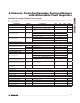
6-Channel, Flash-Configurable System Manager with Nonvolatile Fault Registers FLASH ADDRESS REGISTER ADDRESS READ/ WRITE DESCRIPTION ADC VALUES, FAULT REGISTERS, GPIO_s AS INPUT PORTS—NOT IN FLASH — 000 R MON1 ADC output, MSBs — 001 R MON1 ADC output, LSBs — 002 R MON2 ADC output, MSBs — 003 R MON2 ADC output, LSBs — 004 R MON3 ADC output, MSBs — 005 R MON3 ADC output, LSBs — 006 R MON4 ADC output, MSBs — 007 R MON4 ADC output, LSBs — 008 R MON5 ADC output, MSBs — 00
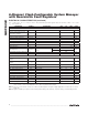
MAX16068 6-Channel, Flash-Configurable System Manager with Nonvolatile Fault Registers Register Map (continued) FLASH ADDRESS REGISTER ADDRESS READ/ WRITE DESCRIPTION ADC—CONVERSIONS 243 043 R/W ADCs voltage ranges for MON_ monitoring 244 044 R/W ADCs voltage ranges for MON_ monitoring 245–247 045–047 — Reserved Reserved INPUT THRESHOLDS 248 048 — 249 049 R/W MON1 OV threshold 24A 04A R/W MON1 UV threshold 24B 04B — 24C 04C R/W MON2 OV threshold 24D 04D R/W MON2 UV thre
6-Channel, Flash-Configurable System Manager with Nonvolatile Fault Registers FLASH ADDRESS REGISTER ADDRESS READ/ WRITE 273 073 R/W 274 074 R/W Watchdog independent mode, MARGIN enabled, soft RESET functionality ADC fault deglitch/autoretry configuration 275 075 R/W WDI toggle/fault timeout, reverse sequencing bit 276 076 R/W WDRESET, WD timers 277 077 R/W Boot-up delay 278 078 — Reserved 279 079 — Reserved 27A 07A — Reserved DESCRIPTION TIMEOUTS 27B 07B — Reserved 2
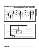
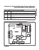
6-Channel, Flash-Configurable System Manager with Nonvolatile Fault Registers MAX16068 Typical Operating Circuit +48V IN OUT IN DC-DC EN LATCH CIRCUIT IN OUT IN DC-DC OUT IN DC-DC MON1 OUT 3.3V DC-DC MON2 MON3– MON6 FAULT VCC RESET MAX16068 SCL EN ABP DBP GND AO SDA Package Information Chip Information For the latest package outline information and land patterns, go to www.maxim-ic.com/packages. Note that a “+”, “#”, or “-” in the package code indicates RoHS status only.