9-5003; Rev 0; 10/09 12-Channel/8-Channel, Flash-Configurable System Monitors with Nonvolatile Fault Registers Features The MAX16070/MAX16071 flash-configurable system monitors supervise multiple system voltages. The MAX16070/MAX16071 can also accurately monitor (Q2.5%) one current channel using a dedicated highside current-sense amplifier. The MAX16070 monitors up to twelve system voltages simultaneously, and the MAX16071 monitors up to eight supply voltages.
MAX16070/MAX16071 12-Channel/8-Channel, Flash-Configurable System Managers with Nonvolatile Fault Registers ABSOLUTE MAXIMUM RATINGS VCC, CSP, CSM to GND.........................................-0.3V to +15V CSP to CSM...........................................................-0.7V to +0.7V MON_, GPIO_, SCL, SDA, A0, RESET to GND (programmed as open-drain outputs)..................-0.3V to +6V EN, TCK, TMS, TDI to GND.....................................-0.3V to +4V DBP, ABP to GND....-0.
12-Channel/8-Channel, Flash-Configurable System Managers with Nonvolatile Fault Registers (VCC = 2.8V to 14V, TA = -40NC to +85NC, unless otherwise specified. Typical values are at ABP = DBP = VCC = 3.3V, TA = +25NC.) (Note 1) PARAMETER SYMBOL CONDITIONS MIN TYP MAX UNITS Bits LSB ADC DC ACCURACY Resolution Gain Error ADCGAIN Offset Error ADCOFF 10 0.35 0.
MAX16070/MAX16071 12-Channel/8-Channel, Flash-Configurable System Managers with Nonvolatile Fault Registers ELECTRICAL CHARACTERISTICS (continued) (VCC = 2.8V to 14V, TA = -40NC to +85NC, unless otherwise specified. Typical values are at ABP = DBP = VCC = 3.3V, TA = +25NC.) (Note 1) PARAMETER SYMBOL CONDITIONS MIN TYP MAX UNITS OUTPUTS (RESET, GPIO_) ISINK = 2mA 0.4 ISINK = 10mA, GPIO_ only 0.7 VCC = 1.2V, ISINK = 100μA (RESET only) 0.
12-Channel/8-Channel, Flash-Configurable System Managers with Nonvolatile Fault Registers (VCC = 2.8V to 14V, TA = -40NC to +85NC, unless otherwise specified. Typical values are at ABP = DBP = VCC = 3.3V, TA = +25NC.) (Note 1) PARAMETER SYMBOL Output Fall Time tOF Data Hold Time tHD:DAT Pulse Width of Spike Suppressed CONDITIONS MIN TYP CBUS = 10pF to 400pF From 50% SCL falling to SDA change 0.3 tSP MAX UNITS 250 ns 0.
MAX16070/MAX16071 12-Channel/8-Channel, Flash-Configurable System Managers with Nonvolatile Fault Registers SDA tSU:DAT tHD:DAT tLOW tBUF tSU:STA tHD:STA tSU:STO SCL tHIGH tHD:STA tR tF START CONDITION STOP CONDITION REPEATED START CONDITION Figure 1. SMBus Timing Diagram t1 t2 t3 TCK t4 t5 TDI, TMS t6 t7 TDO Figure 2.
12-Channel/8-Channel, Flash-Configurable System Managers with Nonvolatile Fault Registers NORMALIZED MON_ THRESHOLD vs. TEMPERATURE +25NC 3 -40NC ABP AND DBP REGULATORS ACTIVE 2 FOR LOW-VOLTAGE APPLICATIONS VCC < 3.6V CONNECT ABP AND DBP TO VCC 1 0 2 4 6 8 10 5.6V RANGE, HALF SCALE, PUV THRESHOLD 0.2 -40 -20 0 20 40 60 MAX16070 toc03 1.002 1.000 0.998 0.996 0.994 0 0.992 80 -40 -20 0 20 40 60 VCC (V) TEMPERATURE (NC) TEMPERATURE (NC) TRANSIENT DURATION vs.
Typical Operating Characteristics (continued) (Typical values are at VCC = 3.3V, TA = +25°C, unless otherwise noted.) INTEGRAL NONLINEARITY vs. CODE DIFFERENTIAL NONLINEARITY vs. CODE 0.6 0.8 0.6 0.4 0.2 0.2 DNL (LSB) 0.4 0 -0.2 0 -0.2 -0.4 -0.4 -0.6 -0.6 -0.8 -0.8 -1.0 -1.0 128 256 384 512 640 768 896 1024 0 128 256 384 512 640 768 896 1024 CODE (LSB) CODE (LSB) NORMALIZED CURRENT-SENSE ACCURACY vs. TEMPERATURE CURRENT-SENSE ACCURACY vs. CSP-CSM VOLTAGE 1.0 MAX16070 toc12 1.05 1.
12-Channel/8-Channel, Flash-Configurable System Managers with Nonvolatile Fault Registers PIN NAME FUNCTION MAX16070 MAX16071 1–5, 34, 35, 40 1–5, 37, 38, 40 MON2–MON6, MON7, MON8, MON1 6 6 CSP Current-Sense Amplifier Positive Input. Connect CSP to the source side of the external sense resistor. 7 7 CSM Current-Sense Amplifier Negative Input. Connect CSM to the load side of the external sense resistor. 8 8 RESET Monitor Voltage Input 1–Monitor Voltage Input 8.
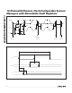
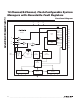
MAX16070/MAX16071 12-Channel/8-Channel, Flash-Configurable System Managers with Nonvolatile Fault Registers Functional Diagram VCC ABP DBP OVERC RESET MAX16070 MAX16071 ANYFAULT FAULT1 DECODE LOGIC FAULT2 MR EN MARGIN 1.
12-Channel/8-Channel, Flash-Configurable System Managers with Nonvolatile Fault Registers The MAX16070 monitors up to twelve system power supplies and the MAX16071 can monitor up to eight system power supplies. After boot-up, if EN is high and the software enable bit is set to ‘1,’ monitoring begins based on the configuration stored in flash. An internal multiplexer cycles through each MON_ input.
MAX16070/MAX16071 12-Channel/8-Channel, Flash-Configurable System Managers with Nonvolatile Fault Registers When in the monitoring state, a register bit, ENRESET, is set to a ‘1’ when EN falls below the undervoltage threshold. This register bit latches and must be cleared through software. This bit indicates if RESET asserted low due to EN going under the threshold. The POR state of ENRESET is ‘0’. The bit is only set on a falling edge of the EN comparator output or the software enable bit.
12-Channel/8-Channel, Flash-Configurable System Managers with Nonvolatile Fault Registers Internal Current-Sense Amplifier The current-sense inputs, CSP/CSM, and a currentsense amplifier facilitate power monitoring (see Figure 4). The voltage on CSP relative to GND is also monitored by the ADC when the current-sense amplifier is enabled with r47h[0]. The conversion results are located in registers r19h and r1Ah (see Table 6). There are two selectable voltage ranges for CSP set by r47h[1], see Table 4.
MAX16070/MAX16071 12-Channel/8-Channel, Flash-Configurable System Managers with Nonvolatile Fault Registers Table 4.
12-Channel/8-Channel, Flash-Configurable System Managers with Nonvolatile Fault Registers REGISTER ADDRESS 44h 45h FLASH ADDRESS BIT RANGE DESCRIPTION [1:0] ADC5 full-scale range 00 = 5.6V 01 = 2.8V 10 = 1.4V 11 = Channel not converted [3:2] ADC6 full-scale range 00 = 5.6V 01 = 2.8V 10 = 1.4V 11 = Channel not converted [5:4] ADC7 full-scale range 00 = 5.6V 01 = 2.8V 10 = 1.4V 11 = Channel not converted [7:6] ADC8 full-scale range 00 = 5.6V 01 = 2.8V 10 = 1.
MAX16070/MAX16071 12-Channel/8-Channel, Flash-Configurable System Managers with Nonvolatile Fault Registers Table 5.
12-Channel/8-Channel, Flash-Configurable System Managers with Nonvolatile Fault Registers REGISTER ADDRESS BIT RANGE DESCRIPTION 00h [7:0] ADC1 result (MSB) bits 9–2 01h [7:6] ADC1 result (LSB) bits 1, 0 02h [7:0] ADC2 result (MSB) bits 9–2 03h [7:6] ADC2 result (LSB) bits 1, 0 04h [7:0] ADC3 result (MSB) bits 9–2 05h [7:6] ADC3 result (LSB) bits 1, 0 06h [7:0] ADC4 result (MSB) bits 9–2 07h [7:6] ADC4 result (LSB) bits 1, 0 08h [7:0] ADC5 result (MSB) bits 9–2 09h [7:6] ADC5
MAX16070/MAX16071 12-Channel/8-Channel, Flash-Configurable System Managers with Nonvolatile Fault Registers General-Purpose Inputs/Outputs GPIO1 to GPIO8 are programmable general-purpose inputs/outputs. GPIO1–GPIO8 are configurable as a manual reset input, a watchdog timer input and output, logic inputs/outputs, fault-dependent outputs. When programmed as outputs, GPIO_s are open drain or pushpull. See Tables 8 and 9 for more detailed information on configuring GPIO1 to GPIO8.
12-Channel/8-Channel, Flash-Configurable System Managers with Nonvolatile Fault Registers REGISTER ADDRESS FLASH ADDRESS BIT RANGE [0] [1] [2] [3] 42h 242h [4] [5] [6] [7] MAX16070/MAX16071 Table 8.
MAX16070/MAX16071 12-Channel/8-Channel, Flash-Configurable System Managers with Nonvolatile Fault Registers Fault1 and Fault2 GPIO1 to GPIO8 are configurable as dedicated fault outputs, Fault1 or Fault2. Fault outputs can assert on one or more overvoltage, undervoltage, or early warning conditions for selected inputs, as well as the secondary overcurrent comparator. Fault1 and Fault2 dependencies are set using registers r36h to r3Ah. See Table 10.
12-Channel/8-Channel, Flash-Configurable System Managers with Nonvolatile Fault Registers REGISTER ADDRESS 39h 3Ah FLASH ADDRESS BIT RANGE [0] 1 = Fault2 depends on MON9 [1] 1 = Fault2 depends on MON10 [2] 1 = Fault2 depends on MON11 [3] 1 = Fault2 depends on MON12 [4] 1 = Fault2 depends on the overvoltage thresholds of the inputs selected by r38h and r39h[3:0] [5] 1 = Fault2 depends on the undervoltage thresholds of the inputs selected by r38h and r39h[3:0] [6] 1 = Fault2 depends on the ea
MAX16070/MAX16071 12-Channel/8-Channel, Flash-Configurable System Managers with Nonvolatile Fault Registers Table 11.
12-Channel/8-Channel, Flash-Configurable System Managers with Nonvolatile Fault Registers Deglitch Fault conditions are detected at the end of each conversion. When the voltage on an input falls outside a monitored threshold for one acquisition, the input multiplexer remains on that channel and performs several successive conversions.
MAX16070/MAX16071 12-Channel/8-Channel, Flash-Configurable System Managers with Nonvolatile Fault Registers Table 14.
12-Channel/8-Channel, Flash-Configurable System Managers with Nonvolatile Fault Registers REGISTER ADDRESS 72h FLASH ADDRESS BIT RANGE 272h DESCRIPTION [0] 1 = Fault log triggered when MON9 is above/below the early threshold warning [1] 1 = Fault log triggered when MON10 is above/below the early threshold warning [2] 1 = Fault log triggered when MON11 is above/below the early threshold warning [3] 1 = Fault log triggered when MON12 is above/below the early threshold warning [4] 1 = Fault log
MAX16070/MAX16071 12-Channel/8-Channel, Flash-Configurable System Managers with Nonvolatile Fault Registers Table 15.
12-Channel/8-Channel, Flash-Configurable System Managers with Nonvolatile Fault Registers REGISTER ADDRESS FLASH ADDRESS BIT RANGE [1:0] 3Bh 0 = Active-low 1 = Active-high [3] 0 = Push-pull 1 = Open drain 23Bh 3Dh 23Ch 23Dh Reset output depends on: 00 = Undervoltage threshold violations 01 = Early warning threshold violations 10 = Overvoltage threshold violations 11 = Undervoltage or overvoltage threshold violations [2] [7:4] 3Ch DESCRIPTION Reset timeout period 0000 = 25μs 0001 = 1.
MAX16070/MAX16071 12-Channel/8-Channel, Flash-Configurable System Managers with Nonvolatile Fault Registers Table 17.
12-Channel/8-Channel, Flash-Configurable System Managers with Nonvolatile Fault Registers MAX16070/MAX16071 VTH LAST MON_ < tWDI tWDI_STARTUP WDI < tWDI tRP RESET Figure 5. Normal Watchdog Startup Sequence VCC WDI < tWDI < tWDI > tWDI < tWDI < tWDI < tWDI < tWDI 0V tWDI VCC WDO 0V Figure 6. Watchdog Timer Operation VCC < tWDI WDI tWDI tRP < tWDI_STARTUP < tWDI 0V VCC RESET 0V VCC WDO 0V 1µs Figure 7.
MAX16070/MAX16071 12-Channel/8-Channel, Flash-Configurable System Managers with Nonvolatile Fault Registers Independent Watchdog Timer Operation When r73h[3] is ‘1’ the watchdog timer operates in the independent mode. In the independent mode, the watchdog timer operates as if it were a separate device. The watchdog timer is activated immediately upon VCC exceeding UVLO and once the boot-up sequence is finished. When RESET is asserted, the watchdog timer and WDO are not affected.
12-Channel/8-Channel, Flash-Configurable System Managers with Nonvolatile Fault Registers SDA SCL SCL DATA LINE STABLE, CHANGE OF DATA ALLOWED DATA VALID S P START CONDITION STOP CONDITION Figure 8. Bit Transfer Figure 9. START and STOP Conditions Bit Transfer Each clock pulse transfers one data bit. The data on SDA must remain stable while SCL is high (Figure 8); otherwise the MAX16070/MAX16071 register a START or STOP condition (Figure 9) from the master.
MAX16070/MAX16071 12-Channel/8-Channel, Flash-Configurable System Managers with Nonvolatile Fault Registers CLOCK PULSE FOR ACKNOWLEDGE 2 1 SCL 8 9 SDA BY TRANSMITTER S NACK SDA BY RECEIVER ACK Figure 10. Acknowledge Table 19. SMBus Settings Register REGISTER ADDRESS FLASH ADDRESS 8Bh 28Bh BIT RANGE [6:0] [7] DESCRIPTION I2C Slave Address Register. Set to 00h to use A0 pin address setting. 1 = Enable PEC (packet error check). Table 20.
12-Channel/8-Channel, Flash-Configurable System Managers with Nonvolatile Fault Registers The CRC-8 byte is calculated using the polynomial C = X8 + X2 + X + 1 The PEC calculation includes all bytes in the transmission, including address, command, and data. The PEC calculation does not include ACK, NACK, START, STOP, or REPEATED START. Command Codes The MAX16070/MAX16071 use eight command codes for block read, block write, and other commands. See Table 21 for a list of command codes.
MAX16070/MAX16071 12-Channel/8-Channel, Flash-Configurable System Managers with Nonvolatile Fault Registers Send Byte Format S ADDRESS Receive Byte Format R/W ACK 7 bits 0 0 Slave Address: Address of the slave on the serial interface bus. COMMAND ACK 8 bits 0 P ADDRESS S Data Byte: Presets the internal address pointer or represents a command. ADDRESS 7 bits SLAVE ADDRESS 0 DATA NACK 8 bits 1 P Data Byte: Data is read from the location pointed to by the internal address pointer.
12-Channel/8-Channel, Flash-Configurable System Managers with Nonvolatile Fault Registers 7) The slave asserts an ACK on the data line. 8) The master sends an 8-bit PEC byte. 9) The slave asserts an ACK on the data line (if PEC is good, otherwise NACK). 10) The master generates a STOP condition. 2) The master sends the 7-bit slave address and a read bit (high).
MAX16070/MAX16071 12-Channel/8-Channel, Flash-Configurable System Managers with Nonvolatile Fault Registers Block Write The block write protocol (see Figure 11) allows the master device to write a block of data (1 byte to 16 bytes) to memory. Preload the destination address by a previous send byte command; otherwise the block write command begins to write at the current address pointer. After the last byte is written, the address pointer remains preset to the next valid address.
12-Channel/8-Channel, Flash-Configurable System Managers with Nonvolatile Fault Registers REGISTER ADDRESS 35h 3) FLASH ADDRESS 235h BIT RANGE [1:0] DESCRIPTION SMBus Alert Configuration 00 = Disabled 01 = Fault1 is SMBus ALERT 10 = Fault2 is SMBus ALERT 11 = Any_Fault is SMBus ALERT The addressed slave asserts an ACK on the data line. 4) The master sends 8 bits of the block read command code. 5) The slave asserts an ACK on the data line unless busy.
MAX16070/MAX16071 12-Channel/8-Channel, Flash-Configurable System Managers with Nonvolatile Fault Registers REGISTERS AND FLASH 01100 01011 01010 01001 01000 00111 MEMORY WRITE REGISTER [LENGTH = 8 BITS] 00110 MEMORY READ REGISTER [LENGTH = 8 BITS] 00101 MEMORY ADDRESS REGISTER [LENGTH = 8 BITS] 00100 USER CODE REGISTER [LENGTH = 32 BITS] 00011 IDENTIFICATION REGISTER [LENGTH = 32 BITS] BYPASS REGISTER [LENGTH = 1 BIT] MUX 1 00000 11111 COMMAND DECODER 01001 SETFLSHADD 01010 RSTFLSHADD 01
12-Channel/8-Channel, Flash-Configurable System Managers with Nonvolatile Fault Registers TEST-LOGIC-RESET 0 0 RUN-TEST/IDLE 1 SELECT-DR-SCAN 1 SELECT-IR-SCAN 0 1 0 1 CAPTURE-DR CAPTURE-IR 0 0 SHIFT-DR 1 1 EXIT1-DR 1 EXIT1-IR 0 0 PAUSE-DR PAUSE-IR 0 1 0 1 0 EXIT2-DR EXIT2-IR 1 1 UPDATE-DR 1 0 SHIFT-IR 0 1 0 1 UPDATE-IR 0 1 0 Figure 13. Tap Controller State Diagram data register remains at its current value.
MAX16070/MAX16071 12-Channel/8-Channel, Flash-Configurable System Managers with Nonvolatile Fault Registers Exit1-IR: A rising edge on TCK with TMS low puts the controller in the pause-IR state. If TMS is high on the rising edge of TCK, the controller enters the update-IR state. register connects between TDI and TDO. While in the shift-IR state, a rising edge on TCK with TMS low shifts the data one stage toward the serial output at TDO.
12-Channel/8-Channel, Flash-Configurable System Managers with Nonvolatile Fault Registers MSB LSB Don’t Care 00000000000000000 SMBus slave id See Table 20 USERCODE: When the USERCODE instruction latches into the parallel instruction register, the user-code data register is selected. The device user-code loads into the user-code data register on the rising edge of TCK following entry into the capture-DR state. Shift-DR can be used to shift the user-code out serially through TDO. See Table 25.
MAX16070/MAX16071 12-Channel/8-Channel, Flash-Configurable System Managers with Nonvolatile Fault Registers The capacitor value depends on VIN and the time delay required, tFAULT_SAVE. Use the following formula to calculate the capacitor size: across the diode, and VUVLO is 2.7V. For example, with a VIN of 14V, a diode drop of 0.7V, and a tFAULT_SAVE of 153ms, the minimum required capacitance is 202FF.
12-Channel/8-Channel, Flash-Configurable System Managers with Nonvolatile Fault Registers Cascading Multiple MAX16070/MAX16071s Multiple MAX16070/MAX16071s can be cascaded to increase the number of monitored rails. There are many ways to cascade the devices depending on the desired behavior. In general, there are several techniques: U Configure a GPIO_ on each device to be EXTFAULT (open drain). Externally wire them together with a single pullup resistor.
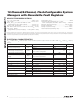
MAX16070/MAX16071 12-Channel/8-Channel, Flash-Configurable System Managers with Nonvolatile Fault Registers Register Map FLASH ADDRESS REGISTER ADDRESS READ/ WRITE DESCRIPTION ADC VALUES, FAULT REGISTERS, GPIO_S AS INPUT PORTS–NOT IN FLASH — 000 R MON1 ADC output, MSBs — 001 R MON1 ADC output, LSBs — 002 R MON2 ADC output, MSBs — 003 R MON2 ADC output, LSBs — 004 R MON3 ADC output, MSBs — 005 R MON3 ADC output, LSBs — 006 R MON4 ADC output, MSBs — 007 R MON4 ADC output, L
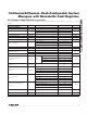
12-Channel/8-Channel, Flash-Configurable System Managers with Nonvolatile Fault Registers FLASH ADDRESS REGISTER ADDRESS READ/ WRITE DESCRIPTION GPIO AND OUTPUT DEPENDENCIES/CONFIGURATIONS 230 030 R/W Reserved 231 031 R/W Reserved 232 032 R/W Reserved 233 033 R/W Reserved 234 034 R/W Reserved 235 035 R/W SMBALERT pin configuration 236 036 R/W Fault1 dependencies 237 037 R/W Fault1 dependencies 238 038 R/W Fault2 dependencies 239 039 R/W Fault2 dependencies 23A 03
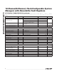
MAX16070/MAX16071 12-Channel/8-Channel, Flash-Configurable System Managers with Nonvolatile Fault Registers Register Map (continued) FLASH ADDRESS REGISTER ADDRESS READ/ WRITE 254 054 R/W MON5 secondary selectable UV/OV 255 055 R/W MON5 primary OV 256 056 R/W MON5 primary UV 257 057 R/W MON6 secondary selectable UV/OV 258 058 R/W MON6 primary OV 259 059 R/W MON6 primary UV 25A 05A R/W MON7 secondary selectable UV/OV 25B 05B R/W MON7 primary OV 25C 05C R/W MON7 primary
12-Channel/8-Channel, Flash-Configurable System Managers with Nonvolatile Fault Registers FLASH ADDRESS REGISTER ADDRESS READ/ WRITE 278 078 R/W Reserved 279 079 R/W Reserved 27A 07A R/W Reserved 27B 07B R/W Reserved 27C 07C R/W Reserved 27D 07D R/W Reserved 27E 07E R/W Reserved 27F 07F R/W Reserved 280 080 R/W Reserved 281 081 R/W Reserved 282 082 R/W Reserved 283 083 R/W Reserved 284 084 R/W Reserved 285 085 R/W Reserved 286 086 R/W Reserved 2
MAX16070/MAX16071 12-Channel/8-Channel, Flash-Configurable System Managers with Nonvolatile Fault Registers Register Map (continued) FLASH ADDRESS REGISTER ADDRESS READ/ WRITE DESCRIPTION USER FLASH 300 39F R/W User flash 3A0 3AF — Reserved 3B0 3FF R/W User flash Typical Operating Circuits VSUPPLY +3.
12-Channel/8-Channel, Flash-Configurable System Managers with Nonvolatile Fault Registers VSUPPLY +3.
GPIO3 GPIO4 GPIO5 GPIO6 N.C. N.C. N.C. EN TOP VIEW N.C. DBP Pin Configurations 30 29 28 27 26 25 24 23 22 21 VCC 31 20 GPIO2 ABP 32 19 GPIO1 GND 33 18 GPIO8 MON7 34 17 GPIO7 16 GND MON8 35 MAX16070 MON9 36 15 SCL 14 AO MON10 37 MON11 38 13 SDA *EP + MON12 39 12 TDO 11 TCK TDI 10 TMS 9 GPIO6 8 GPIO5 MON5 7 RESET MON4 6 N.C. MON3 5 CSM 4 N.C. 3 CSP 2 MON6 1 MON2 MON1 40 N.C. N.C. N.C. N.C. EN N.C.
12-Channel/8-Channel, Flash-Configurable System Managers with Nonvolatile Fault Registers PROCESS: BiCMOS Package Information For the latest package outline information and land patterns, go to www.maxim-ic.com/packages. Note that a “+”, “#”, or “-” in the package code indicates RoHS status only. Package drawings may show a different suffix character, but the drawing pertains to the package regardless of RoHS status. PACKAGE TYPE PACKAGE CODE DOCUMENT NO.