
Manual


MAX1684/MAX1685
Low-Noise, 14V Input, 1A, PWM
Step-Down Converters
______________________________________________________________________________________ 11
The output current capability for each mode is deter-
mined by the following equations:
I
OUTMAX
= I
LIM
- 0.5
✕
I
RIPPLE
(for PWM and normal
modes)
I
OUTMAX
= 0.5
✕
I
LIMLP
(for low-power mode)
where:
I
RIPPLE
= ripple current = (V
IN
- V
OUT
)
✕
V
OUT
/ (V
IN
✕
f
OSC
✕
L)
I
LIM
= current limit in PWM mode
I
LIMLP
= current limit in low-power mode
Internal Low-Voltage Regulators and
Bootstrap (BOOT)
The MAX1684/MAX1685 have two internal regulators
(VH and VL) that generate low-voltage supplies for
internal circuitry (see the Functional Diagram). The VH
regulator generates -4.6V with respect to IN to supply
the P-channel switch and driver. Bypass CVH to IN with
a 0.1µF capacitor. The VL regulator generates a 3V out-
put at CVL to supply internal low-voltage blocks, as well
as the N-channel switch and driver. Bypass CVL to
AGND with a 1µF capacitor.
To reduce the quiescent current in low-power and nor-
mal modes, connect BOOT to OUT. After startup, when
V
BOOT
exceeds 2.6V, the internal bootstrap switch con-
nects CVL to BOOT. This bootstrap mechanism causes
the internal circuitry to be supplied from the output and
thereby reduces the input quiescent current by a factor
of V
OUT
/ V
IN
. Do not connect BOOT to OUT if the out-
put voltage exceeds 5.5V. Instead, connect BOOT to
AGND to keep CVL regulated at 3V.
CVL has a 5mA capability to supply external logic cir-
cuitry and is disabled in shutdown mode.
Applications Information
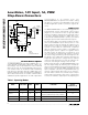
Output Voltage Selection
Connect FB to AGND to select the internal 3.3V output
mode. Connect BOOT to OUT in this configuration.
To select an output voltage between 1.25V and V
IN
,
connect FB to a resistor voltage-divider between the
output and AGND (Figure 3). Select R2 in the 20kΩ to
100kΩ range. Calculate R1 as follows:
R1 = R2 [( V
OUT
/ V
FB
) - 1]
where V
FB
= 1.25V.
Connect a small capacitor across R1 to compensate for
stray capacitance at the FB pin:
where: R2 = 100kΩ, use 4.7pF.
Inductor Selection
The MAX1684/MAX1685s’ high switching frequency
allows the use of small surface-mount inductors. Table 2
shows a selection of suitable inductors for different out-
put voltage ranges. Calculate the minimum inductor by:
L = 0.9(V
OUT
- 0.3V) / (I
RIPPLE MAX
× f
OSC
)
where:
I
RIPPLE MAX
= should be less than or equal to 400mA
f
OSC
= 300kHz (MAX1684) or 600kHz (MAX1685)
Capacitor Selection
Select input and output filter capacitors to service
inductor currents while minimizing voltage ripple. The
input filter capacitor reduces peak currents and noise
at the voltage source. The MAX1684/MAX1685s’ loop
gain is relatively low to enable the use of small, low-
value output filter capacitors. Higher capacitor values
provide improved output ripple and transient response.
Low-ESR capacitors are recommended. Capacitor ESR
is a major contributor to output ripple (usually more
than 60%). Avoid ordinary aluminum electrolytic capac-
itors, as they typically have high ESR. Low-ESR alu-
minum electrolytic capacitors are acceptable and
relatively inexpensive. Low-ESR tantalum capacitors
are better and provide a compact solution for space-
constrained surface-mount designs. Do not exceed the
ripple-current ratings of tantalum capacitors. Ceramic
capacitors offer the lowest ESR overall. Sanyo OS-CON
C1
5 (10
R
7
2
=
−
)
MAX1684
MAX1685
FB
V
OUT
R1 C1
R2
Figure 3. Setting Output Voltage