
Manual

MAX1684/MAX1685
Low-Noise, 14V Input, 1A, PWM
Step-Down Converters
2 _______________________________________________________________________________________
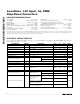
ABSOLUTE MAXIMUM RATINGS
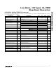
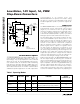
ELECTRICAL CHARACTERISTICS
(V
IN
= V
SHDN
= 6V, STBY = SYNC/PWM = CVL, V
BOOT
= V
OUT
, FB = AGND, circuit of Figure 1, T
A
= 0°C to +85°C, unless otherwise
noted. Typical values are at T
A
= +25°C.)
Stresses beyond those listed under “Absolute Maximum Ratings” may cause permanent damage to the device. These are stress ratings only, and functional
operation of the device at these or any other conditions beyond those indicated in the operational sections of the specifications is not implied. Exposure to
absolute maximum rating conditions for extended periods may affect device reliability.
AIN to AGND ............................................................-0.3 to +15V
IN to PGND ................................................-0.3V to (V
AIN
+ 0.3V)
LX to PGND .................................................-0.5V to (V
IN
+ 0.3V)
PGND to AGND ..................................................................±0.3V
SHDN to AGND .........................................-0.3V to (V
AIN
+ 0.3V)
ILIM/SS, FB, CC, BOOT, REF to AGND ....-0.3V to (V
CVL
+ 0.3V)
CVH to IN..................................................................-6V to +0.3V
CVL, STBY, SYNC/PWM to AGND............................-0.3V to +6V
Reference Current ..............................................................±1mA
CVL Current .......................................................-1mA to +10mA
LX Peak Current (Internally Limited) .....................................2.3A
Continuous Power Dissipation (T
A
= +70°C)
16-Pin QSOP (derate 8.3mW/°C above +70°C)............667mW
Operating Temperature Range ...........................-40°C to +85°C
Junction Temperature......................................................+150°C
Storage Temperature Range .............................-65°C to +150°C
Lead Temperature (soldering, 10s) .................................+300°C
V
FB
= V
OUT
, I
LOAD
= 0 to 1A
Low-power mode, STBY = low,
V
BOOT
= 3.3V (Note 2)
Normal mode, SYNC/PWM = low,
V
BOOT
= 3.3V (Note 2)
PWM mode,
SYNC/PWM = high,
V
BOOT
= 3.3V
(Note 2)
SYNC/PWM = high
Low-side switch, V
IN
= 2.7V, I
LX
= 200mA
High-side switch,
I
LX
= 1A
V
FB
= V
OUT
, I
LOAD
= 0 to 1A
V
IN
= 5V to 14V
BOOT = AGND (Note 1)
SYNC/PWM = low
V
FB
= 1.4V
CONDITIONS
0.14 0.27
Quiescent Power Consumption
0.9 2
25 65
mW
13 33
mA
20 80 130
Zero Crossing Threshold
-10 50 100
VV
FB
Feedback Voltage 1.238 1.251 1.264
V2.7 14Input Voltage Range
A0.15 0.4 0.9Current Limit, N-Channel
A1.2 1.75 2.3I
LIM
Current Limit in PWM Mode
Ω38On-Resistance, N-Channel
0.24 0.5
%0.01Output Load Regulation
A1Output Current Capability
VV
REF
V
IN
Output Adjust Range
nA-50 50I
FB
FB Input Current
UNITSMIN TYP MAXSYMBOLPARAMETER
FB = AGND, I
LOAD
= 0 to 1A VV
OUT
Output Voltage (3.3V Mode) 3.296 3.333 3.368
V
IN
= 6V
V
IN
= 2.7V
Ω
0.34 0.8
On-Resistance, P-Channel
MAX1684
MAX1685
MAX1684
MAX1685
SYNC/PWM = low mA285 380 475Pulse-Skipping Current Threshold
STBY = low
mA285 380 475I
LIMLP
Current Limit in Low-Power
Mode