
User guide
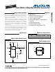

MAX17067
Low-Noise Step-Up DC-DC Converter
10 ______________________________________________________________________________________
Diode Selection
The output diode should be rated to handle the output
voltage and the peak switch current. Make sure that the
diode’s peak current rating is at least I
PK
and that its
breakdown voltage exceeds V
OUT
. Schottky diodes are
recommended.
Input and Output Capacitor Selection
Low-ESR capacitors are recommended for input
bypassing and output filtering. Low-ESR tantalum
capacitors are a good compromise between cost and
performance. Ceramic capacitors are also a good
choice. Avoid standard aluminum electrolytic capaci-
tors. A simple equation to estimate input and output-
capacitor values for a given voltage ripple is as follows:
where V
RIPPLE
is the peak-to-peak ripple voltage on the
capacitor.
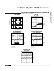
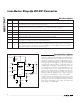
Output Voltage
The MAX17067 operates with an adjustable output from
V
IN
to 20V. Connect a resistor voltage-divider to FB
(see the
Typical Operating Circuit
) from the output to
GND. Select the resistor values as follows:
where V
FB
, the boost-regulator feedback set point, is
1.24V. Since the input bias current into FB is typically
zero, R2 can have a value up to 100kΩ without sacrificing
accuracy. Connect the resistor-divider as close to the IC
as possible.
Loop Compensation
The voltage feedback loop needs proper compensation
to prevent excessive output ripple and poor efficiency
caused by instability. This is done by connecting a resis-
tor (R
COMP
) and capacitor (C
COMP
) in series from
COMP to GND, and another capacitor (C
COMP2
) from
COMP to GND. R
COMP
is chosen to set the high-fre-
quency integrator gain for fast-transient response, while
C
COMP
is chosen to set the integrator zero to maintain
loop stability. The second capacitor, C
COMP2
, is chosen
to cancel the zero introduced by output-capacitance
ESR. For optimal performance, choose the components
using the following equations:
R
COMP
= (274Ω/A
2
x
V
IN
x
V
OUT
x C
OUT
/(L x I
OUT
)
C
COMP
≅ (0.36 x 10
-3
A/Ω) x L/V
IN
C
COMP2
≅ (0.0036 A/Ω) x R
ESR
x L x I
OUT
/(V
IN
x
V
OUT
)
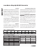
For the ceramic output capacitor, where ESR is small,
C
COMP2
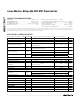
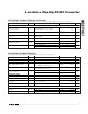
is optional. Table 1 shows experimentally verified
external component values for several applications.
The best gauge of correct loop compensation is by
inspecting the transient response of the MAX17067.
Adjust R
COMP
and C
COMP
as necessary to obtain opti-
mal transient performance.
Soft-Start Capacitor
The soft-start capacitor should be large enough that it
does not reach final value before the output has
reached regulation. Calculate C
SS
to be:
where:
C
OUT
= total output capacitance including any bypass
capacitor on the output bus
V
OUT
= maximum output voltage
I
INRUSH
= peak inrush current allowed
I
OUT
= maximum output current during power-up stage
V
IN
= minimum input voltage
The load must wait for the soft-start cycle to finish
before drawing a significant amount of load current.
The duration after which the load can begin to draw
maximum load current is:
t
MAX
= 2.5 x 10
5
C
SS
C 21 10 C
V
V V
V I I V
SS
6
OUT
IN OUT
IN INRUSH OUT OUT
OUT
2
>× ×
−×
×−×
⎛
⎝
⎜
⎞
⎠
⎟
−
RR
V
V
OUT
FB
12 1=−
⎛
⎝
⎜
⎞
⎠
⎟
C
0.5 L I
V V
PK
2
RIPPLE OUT
≥
××
⎛
⎝
⎞
⎠
×