
User guide


MAX17067
Low-Noise Step-Up DC-DC Converter
______________________________________________________________________________________ 11
Application Circuits
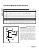
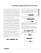
1-Cell to 3.3V SEPIC Power Supply
Figure 3 shows the MAX17067 in a single-ended primary
inductance converter (SEPIC) topology. This topology is
useful when the input voltage can be either higher or
lower than the output voltage, such as when converting
a single lithium-ion (Li+) cell to a 3.3V output. L1A and
L1B are two windings on a single inductor. The coupling
capacitor between these two windings must be a low-
ESR type to achieve maximum efficiency, and must also
be able to handle high ripple currents. Ceramic capaci-
tors are best for this application. The circuit in Figure 3
provides 400mA output current at 3.3V output when
operating with an input voltage from +2.6V to +4.0V.
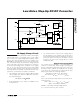
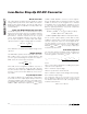
AMLCD Application
Figure 4 shows a power supply for active matrix (TFT-
LCD) flat-panel displays. Output-voltage transient per-
formance is a function of the load characteristic. Add or
remove output capacitance (and recalculate compen-
sation-network component values) as necessary to
meet transient performance. Regulation performance
for secondary outputs (VGOFF and VGON) depends on
the load characteristics of all three outputs.
LX
FB
C6
OPEN
C15
27nF
R2
44.2kΩ
R1
274kΩ
FREQ
IN
V
IN
2.6V TO 4.0V
V
OUT
+9V/250mA
COMP
SHDN
SS
D1
GND
U1
MAX17067
C5
620pF
R5
121kΩ
C1
10μF
10V
R3
10Ω
C4
1μF
R6
100kΩ
L1
3.3μH
6
4
5
2
1
3
7
8
C14
4.7μF
C13
1μF
C12
1μF
D4 D2
1
3
2
2
1
C9
0.1μF
C11
0.1μF
VGOFF
-9V
VGON
+27V
3
C7
10μF
25V
D3
2
1
C10
0.1μF
3
Figure 4. Multiple-Output, Low-Profile (1.2mm max) TFT-LCD Power Supply
LX
IN
V
IN
2.6V TO 4.0V
GND
L1 = CTX8-1P
C
OUT
= TPSD226025R0200
C2
10μF
FREQ
V
OUT
3.3V
CC
SS
SHDN
FB
D1
R1
1MΩ
R2
605kΩ
L1A
5.3μH
0.027μF
MAX17067
C
OUT
22μF
20V
C1
10μF
10V
R
COMP
C
COMP
C
COMP2
L1B
5.3μH
Figure 3. MAX17067 in a SEPIC Configuration