
User guide


MAX17067
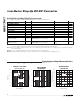
Layout Procedure
Good PCB layout and routing are required in high-fre-
quency switching power supplies to achieve good regu-
lation, high efficiency, and stability. It is strongly
recommended that the evaluation kit PCB layouts be fol-
lowed as closely as possible. Place power components
as close together as possible, keeping their traces short,
direct, and wide. Avoid interconnecting the ground pins
of the power components using vias through an internal
ground plane. Instead, keep the power components
close together and route them in a star ground configura-
tion using component-side copper, then connect the star
ground to internal ground using multiple vias.
Low-Noise Step-Up DC-DC Converter
12 ______________________________________________________________________________________
Chip Information
TRANSISTOR COUNT: 3657