
User guide
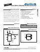
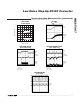
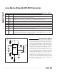
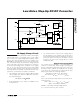

MAX17067
Low-Noise Step-Up DC-DC Converter
2 _______________________________________________________________________________________
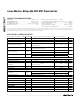
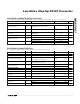
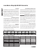
ABSOLUTE MAXIMUM RATINGS
ELECTRICAL CHARACTERISTICS
(V
IN
= SHDN = 3V, FREQ = 3V, T
A
= 0°C to +85°C, unless otherwise noted. Typical values are at T
A
= +25°C.) (Note 2)
Stresses beyond those listed under “Absolute Maximum Ratings” may cause permanent damage to the device. These are stress ratings only, and functional
operation of the device at these or any other conditions beyond those indicated in the operational sections of the specifications is not implied. Exposure to
absolute maximum rating conditions for extended periods may affect device reliability.
LX to GND ..............................................................-0.3V to +22V
SHDN, FREQ to GND ............................................-0.3V to +7.5V
IN to GND (Note 1) ...................................................-0.3V to +6V
SS, COMP, FB to GND ................................-0.3V to (V
IN
+ 0.3V)
RMS LX Pin Current ..............................................................1.2A
Continuous Power Dissipation (T
A
= +70°C)
8-Pin μMAX (derate 4.1mW/°C above +70°C) ............330mW
Operating Temperature Range ...........................-40°C to +85°C
Junction Temperature......................................................+150°C
Storage Temperature Range .............................-65°C to +150°C
Lead Temperature (soldering, 10s) .................................+300°C
PARAMETER SYMBOL CONDITIONS MIN TYP MAX UNITS
Input Supply Range V
IN
V
OUT
< 18V 2.6 4.0 V
Output Voltage 18 V
Input Supply Clamp Voltage
Use external limiting resistor; R
IN
= 100,
V
IN
= 10V (Note 3)
6.05 6.40 6.60 V
V
IN
Undervoltage Lockout UVLO
V
IN
rising, typical hysteresis is 50mV, LX
remains off below this level
2.30 2.45 2.57 V
V
FB
= 1.3V, not switching 0.3 0.6
Quiescent Current I
IN
V
FB
= 1.0V, switching 1.5 2.5
mA
SHDN = GND, T
A
= +25°C 30 60
Shutdown Supply Current I
IN
SHDN = GND, T
A
= +85°C 30
μA
ERROR AMPLIFIER
Feedback Voltage V
FB
Level to produce V
COMP
= 1.24V 1.23 1.24 1.25 V
FB Input Bias Current I
FB
V
FB
= 1.24V 50 125 200 nA
Feedback-Voltage Line
Regulation
Level to produce V
COMP
= 1.24V,
2.6V < V
IN
< 5.5V
0.05 0.15 %/V
Transconductance g
m
I = 5μA 100 240 440 μS
Voltage Gain A
V
3800 V/V
OSCILLATOR
FREQ = GND
500 640 780
Frequency f
OSC
FREQ = IN 1000 1200 1400
kHz
Maximum Duty Cycle DC FREQ = GND, FREQ = IN 89 92 95 %
n-CHANNEL SWITCH
Current Limit I
LIM
V
FB
= 1V, duty cycle = 68% (Note 4) 1.8 2.4 3.4 A
On-Resistance R
ON
150 275 m
Leakage Current I
LXOFF
V
LX
= 20V 10 20 μA
Current-Sense Transresistance R
CS
0.2 0.3 0.4 V/A
SOFT-START
Reset Switch Resistance 100
Charge Current V
SS
= 1.2V 2.5 4.5 6.5 μA