
User guide

MAX17067
Low-Noise Step-Up DC-DC Converter
6 _______________________________________________________________________________________
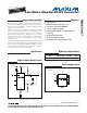
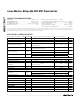
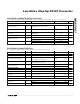
Pin Description
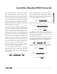
Switch Pin. Connect the inductor/catch diode to LX and minimize the trace area for lowest EMI.LX5
Supply Pin. Bypass IN with at least a 1μF ceramic capacitor directly to GND.IN6
Frequency Select Input. When FREQ is low, the oscillator frequency is set to 640kHz. When FREQ is high,
the frequency is 1.2MHz. This input has a 5μA pulldown current.
FREQ7
Soft-Start Control Pin. Connect a soft-start capacitor (C
SS
) to this pin. Leave open for no soft-start. The soft-
start capacitor is charged with a constant current of 4μA. Full current limit is reached after t = 2.5
x 10
5
C
SS
.
The soft-start capacitor is discharged to ground when SHDN is low. When SHDN goes high, the soft-start
capacitor is charged to 0.5V, after which soft-start begins.
SS8
GroundGND4
Active-Low Shutdown Control Input. Drive SHDN low to turn off the MAX17067. SHDN
3
PIN
Feedback Pin. Reference voltage is 1.24V nominal. Connect an external resistor-divider tap to FB and
minimize the trace area. Set V
OUT
according to: V
OUT
= 1.24V (1 + R1 / R2). See Figure 1.
FB2
Compensation Pin for Error Amplifier. Connect a series RC from COMP to ground. See the
Loop
Compensation
section for component selection guidelines.
COMP1
FUNCTIONNAME
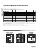
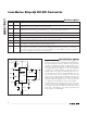
Detailed Description
The MAX17067 is a highly efficient power supply that
employs a current-mode, fixed-frequency PWM architec-
ture for fast-transient response and low-noise operation.
The device regulates the output voltage through a com-
bination of an error amplifier, two comparators, and sev-
eral signal generators (Figure 2). The error amplifier
compares the signal at FB to 1.24V and varies the
COMP output. The voltage at COMP determines the cur-
rent trip point each time the internal MOSFET turns on.
As the load varies, the error amplifier sources or sinks
current to the COMP output accordingly to produce the
inductor peak current necessary to service the load. To
maintain stability at high duty cycle, a slope-compensa-
tion signal is summed with the current-sense signal.
At light loads, this architecture allows the ICs to “skip”
cycles to prevent overcharging the output voltage. In
this region of operation, the inductor ramps up to a fixed
peak value, discharges to the output, and waits until
another pulse is needed again.
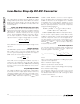
LX
IN
V
IN
2.6V TO 4.0V
GND
FREQ
V
OUT
COMP
SS
SHDN
FB
R1
R2
L
0.027μF
MAX17067
C
OUT
C1
10μF
6.3V
R
COMP
C
COMP
C
COMP2
D1
MBRS130LT1
C
IN
640kHz
1.2MHz
ON/OFF
V
IN
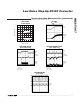
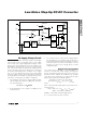
Figure 1. Typical Application Circuit