
User guide
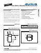

MAX17067
Low-Noise Step-Up DC-DC Converter
_______________________________________________________________________________________ 7
IN Supply Clamp Circuit
The MAX17067 features an internal clamp to allow appli-
cations where there is overvoltage stress on the supply
line. In many cases, high-voltage spikes happen on pro-
duction lines and are difficult to protect against. The
MAX17067’s internal clamp circuit can solve this prob-
lem. The internal clamp circuit limits the voltage at the IN
pin to 6.4V (typ) to protect the IN pin from a continuous
or transient overvoltage stress condition on the supply
line. To use the clamp circuit, put a series resistor (R
IN
)
between supply and IN, and a decoupling capacitor
(1μF typical) from IN to GND. To properly size the exter-
nal resistor, several factors should be considered:
• The maximum current for the clamp is 40mA, and the
clamp voltage at the IN pin is 6.05V (min). Therefore,
the external resistor is:
• Power dissipation in the clamp is in addition to the
total power loss.
• The external resistor causes a DC voltage drop in
the IN supply line. The voltage at the IN pin has to
be properly maintained when clamping is used. The
worst-case quiescent current of the IN pin is 2.5mA;
therefore, the worst-case voltage drop is 2.5mA
multiplied by R
IN
.
Output-Current Capability
The output-current capability of the MAX17067 is a
function of current limit, input voltage, operating fre-
quency, and inductor value. Because of the slope com-
pensation used to stabilize the feedback loop, the duty
cycle affects the current limit. The output-current capa-
bility is governed by the following equation:
I
OUT(MAX)
= [I
LIM
x (1.26 - 0.4 x Duty) -
0.5 x Duty x V
IN
/(f
OSC
x L)] x η x V
IN
/V
OUT
where:
I
LIM
= current limit specified at 68% (see the
Electrical
Characteristics
):
Duty = duty cycle = (V
OUT
- V
IN
+ V
DIODE
)/
(V
OUT
- I
LIM
x R
ON
+ V
DIODE
)
V
DIODE
= catch diode forward voltage at I
LIM
η = conversion efficiency, 85% nominal
RV
IN IN
≥
()
⎡
⎣
⎤
⎦
-605 004..Ω
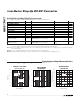
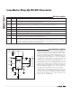
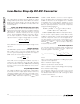
GND
LX
IN
FREQ
FB
COMP
4μA
5μA
N
ERROR
COMPARATOR
ERROR
AMPLIFIER
SKIP
COMPARATOR
SS
CLOCK
SKIP
BIAS
SHDN
MAX17067
Σ
CURRENT
SENSE
CONTROL
AND DRIVER
LOGIC
SOFT-
START
SLOPE
COMPEN-
SATION
OSCILLATOR
∞
1.24V
Figure 2. Functional Diagram