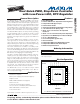
9-4243; Rev 0; 8/08 KIT ATION EVALU E L B A AVAIL Dual Quick-PWM, Step-Down Controller with Low-Power LDO, RTC Regulator *EP = Exposed pad.
MAX17101 Dual Quick-PWM, Step-Down Controller with Low-Power LDO, RTC Regulator ABSOLUTE MAXIMUM RATINGS IN, ONLDO to GND ................................................-0.3V to +28V VDD, VCC to GND .....................................................-0.3V to +6V RTC, LDO to GND ....................................................-0.3V to +6V OUT_ to GND ...........................................................-0.3V to +6V ON1, ON2 to GND....................................................-0.
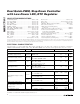
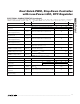
Dual Quick-PWM, Step-Down Controller with Low-Power LDO, RTC Regulator (Circuit of Figure 1, no load on LDO, RTC, OUT1, OUT2, and REF, VIN = 12V, VDD = VCC = VSECFB = 5V, VREFIN2 = 1.0V, BYP = LDOSEL = GND, ONLDO = IN, ON1 = ON2 = VCC, TA = 0°C to +85°C, unless otherwise noted. Typical values are at TA = +25°C.) PARAMETER OUT2 Output-Voltage Accuracy (Note 1) SYMBOL VOUT2 CONDITIONS 3.3V preset output: REFIN2 = VCC (5V), VIN = 12V, SKIP = VCC 1.05V preset output: REFIN2 = RTC (3.
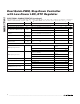
MAX17101 Dual Quick-PWM, Step-Down Controller with Low-Power LDO, RTC Regulator ELECTRICAL CHARACTERISTICS (continued) (Circuit of Figure 1, no load on LDO, RTC, OUT1, OUT2, and REF, VIN = 12V, VDD = VCC = VSECFB = 5V, VREFIN2 = 1.0V, BYP = LDOSEL = GND, ONLDO = IN, ON1 = ON2 = VCC, TA = 0°C to +85°C, unless otherwise noted. Typical values are at TA = +25°C.) PARAMETER LDO Short-Circuit Current SYMBOL I ILIM(LDO) CONDITIONS LDO = GND MIN TYP 100 MAX UNITS 260 mA -6.
Dual Quick-PWM, Step-Down Controller with Low-Power LDO, RTC Regulator (Circuit of Figure 1, no load on LDO, RTC, OUT1, OUT2, and REF, VIN = 12V, VDD = VCC = VSECFB = 5V, VREFIN2 = 1.0V, BYP = LDOSEL = GND, ONLDO = IN, ON1 = ON2 = VCC, TA = 0°C to +85°C, unless otherwise noted. Typical values are at TA = +25°C.
MAX17101 Dual Quick-PWM, Step-Down Controller with Low-Power LDO, RTC Regulator ELECTRICAL CHARACTERISTICS (continued) (Circuit of Figure 1, no load on LDO, RTC, OUT1, OUT2, and REF, VIN = 12V, VDD = VCC = VSECFB = 5V, VREFIN2 = 1.0V, BYP = LDOSEL = GND, ONLDO = IN, ON1 = ON2 = VCC, TA = 0°C to +85°C, unless otherwise noted. Typical values are at TA = +25°C.
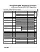
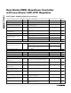
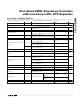
Dual Quick-PWM, Step-Down Controller with Low-Power LDO, RTC Regulator (Circuit of Figure 1, no load on LDO, RTC, OUT1, OUT2, and REF, VIN = 12V, VDD = VCC = VSECFB = 5V, VREFIN2 = 1.0V, BYP = LDOSEL = GND, ONLDO = IN, ON1 = ON2 = VCC, TA = -40°C to +85°C, unless otherwise noted.) (Note 3) PARAMETER SYMBOL CONDITIONS MIN TYP MAX UNITS INPUT SUPPLIES IN Standby Supply Current IIN(STBY) VIN = 6V to 24V, ON1 = ON2 = GND, ONLDO = VCC 200 μA IN Shutdown Supply Current I IN(SHDN) VIN = 4.
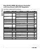
MAX17101 Dual Quick-PWM, Step-Down Controller with Low-Power LDO, RTC Regulator ELECTRICAL CHARACTERISTICS (continued) (Circuit of Figure 1, no load on LDO, RTC, OUT1, OUT2, and REF, VIN = 12V, VDD = VCC = VSECFB = 5V, VREFIN2 = 1.0V, BYP = LDOSEL = GND, ONLDO = IN, ON1 = ON2 = VCC, TA = -40°C to +85°C, unless otherwise noted.) (Note 3) PARAMETER SYMBOL CONDITIONS MIN TYP MAX UNITS LINEAR REGULATOR (LDO) LDO Output-Voltage Accuracy VLDO VIN = 24V, LDOSEL = BYP = GND, 0 < ILDO < 100mA 4.85 5.
Dual Quick-PWM, Step-Down Controller with Low-Power LDO, RTC Regulator (Circuit of Figure 1, no load on LDO, RTC, OUT1, OUT2, and REF, VIN = 12V, VDD = VCC = VSECFB = 5V, VREFIN2 = 1.0V, BYP = LDOSEL = GND, ONLDO = IN, ON1 = ON2 = VCC, TA = -40°C to +85°C, unless otherwise noted.
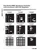
Typical Operating Characteristics (Circuit of Figure 1, VIN = 12V, VDD = VCC = 5V, TON = REF, TA = +25°C, unless otherwise noted.) 80 12V 75 70 65 90 EFFICIENCY (%) 85 PWM MODE 75 70 90 ULTRASONIC MODE 0.1 1 0.1 50 0.1 1 10 SMPS OUTPUT VOLTAGE DEVIATION vs. LOAD CURRENT SWITCHING FREQUENCY vs. LOAD CURRENT PWM MODE 65 60 55 2 1 PWM MODE 0 -1 SKIP MODE -2 12V 50 0.1 1 10 PWM MODE 12V -3 0.01 1000 0.1 0.
Dual Quick-PWM, Step-Down Controller with Low-Power LDO, RTC Regulator STANDBY AND SHUTDOWN INPUT SUPPLY CURRENT vs. INPUT VOLTAGE SUPPLY CURRENT (mA) LDO AND RTC POWER-UP LDO AND RTC POWER REMOVAL MAX17101 toc11 MAX17101 toc10 1 MAX17101 toc12 A 12V B 5V 12V STANDBY (ONLDO = VIN) C 3.3V 0V B 5V 3.3V D 2.0V 0V SHUTDOWN (ONLDO = ON1 = ON2 = GND) A 12V 5V 0V 0.1 12V C 3.3V D 2.0V 2V 0V 0.01 0 INPUT VOLTAGE (V) 200μs/div A. INPUT SUPPLY, 5V/div C. 3.3V RTC, 2V/div B. 5V LDO, 2V/div D.
MAX17101 Dual Quick-PWM, Step-Down Controller with Low-Power LDO, RTC Regulator Typical Operating Characteristics (continued) (Circuit of Figure 1, VIN = 12V, VDD = VCC = 5V, TON = REF, TA = +25°C, unless otherwise noted.) SHUTDOWN WAVEFORMS (SWITCHING REGULATORS) 5V SMPS LOAD TRANSIENT (PWM MODE) MAX17101 toc17 MAX17101 toc16 3.1A 5V A 0V 5V 0V 5V 0V B 0A D 0A A 5V B 0A C C 40μs/div A. LOAD CURRENT, 2A/div B. 5V SMPS OUTPUT, 100mV/div C. INDUCTOR CURRENT, 2A/div 200μs/div A.
Dual Quick-PWM, Step-Down Controller with Low-Power LDO, RTC Regulator PIN NAME FUNCTION REF 2V Reference-Voltage Output. Bypass REF to AGND with a 0.1μF or greater ceramic capacitor. The reference can source up to 50μA for external loads. Loading REF degrades output-voltage accuracy according to the REF load-regulation error (see the Typical Operating Characteristics). The reference shuts down when ON1, ON2, and ONLDO are all pulled low. 2 TON Switching-Frequency Setting Input.
Dual Quick-PWM, Step-Down Controller with Low-Power LDO, RTC Regulator MAX17101 Pin Description (continued) PIN NAME 14 ON1 15 DH1 High-Side Gate-Driver Output for SMPS1. DH1 swings from LX1 to BST1. 16 LX1 Inductor Connection for SMPS1. Connect LX1 to the switched side of the inductor. LX1 is the lower supply rail for the DH1 high-side gate driver. 17 BST1 Boost Flying-Capacitor Connection for SMPS1. Connect to an external capacitor as shown in Figure 1.
Dual Quick-PWM, Step-Down Controller with Low-Power LDO, RTC Regulator INPUT (VIN)* 7V TO 24V C22 0.1μF IN NH1 L1 5V OUTPUT BST2 DH1 BST1 CBST1 0.1μF CIN 4 x 10μF 25V NH2 DH2 CBST2 0.1μF LX2 L2 3.3V OUTPUT COUT2 LX1 DL2 D2 NL2 COUT1 DL1 D1 NL1 PGND RGND 0Ω AGND OUT1 BYP OUT2 DX1 5V SMPS OUTPUT (OUT1) C5 10nF MAX17101 C6 0.1μF C8 0.1μF R4 500kΩ R7 100kΩ } PGOOD1 PGOOD2 C7 10nF 12V TO 15V CHARGE PUMP R6 100kΩ RTC DX2 POWER-GOOD RTC SUPPLY C3 1μF C4 0.
MAX17101 Dual Quick-PWM, Step-Down Controller with Low-Power LDO, RTC Regulator IN ONLDO TON 5V LINEAR REGULATOR SKIP 3.3V LINEAR REGULATOR RTC LDOSEL LDO LDO BYPASS CIRCUITRY BYP SECFB ILIM2 OUT2 ILIM1 VDD OUT1 VDD BST1 PWM1 CONTROLLER (FIGURE 3) DH1 BST2 PWM2 CONTROLLER (FIGURE 3) DH2 LX2 VDD LX1 DL2 VDD DL1 PGND FB SELECT (PRESET vs. ADJ) REFIN2 ON2 FAULT1 ON1 UVLO PGOOD1 FAULT2 FB SELECT (PRESET vs.
Dual Quick-PWM, Step-Down Controller with Low-Power LDO, RTC Regulator COMPONENT Input Voltage 400kHz/300kHz SMPS 1: 5V AT 5A SMPS 2: 3.3V AT 8A 400kHz/500kHz SMPS 1: 5V AT 3A SMPS 2: 3.3V AT 5A MAX17101 Table 1. Component Selection for Standard Applications 400kHz/300kHz SMPS 1: 1.5V AT 8A SMPS 2: 1.
MAX17101 Dual Quick-PWM, Step-Down Controller with Low-Power LDO, RTC Regulator Detailed Description The MAX17101 step-down controller is ideal for highvoltage, low-power supplies for notebook computers. Maxim’s Quick-PWM pulse-width modulator in the MAX17101 is specifically designed for handling fast load steps while maintaining a relatively constant operating frequency and inductor operating point over a wide range of input voltages.
Dual Quick-PWM, Step-Down Controller with Low-Power LDO, RTC Regulator The Quick-PWM control architecture is a pseudo-fixedfrequency, constant on-time, current-mode regulator with voltage feed-forward. This architecture relies on the output filter capacitor’s ESR to act as a currentsense resistor, so the feedback ripple voltage provides the PWM ramp signal.
MAX17101 Dual Quick-PWM, Step-Down Controller with Low-Power LDO, RTC Regulator INTEGRATOR REF GND FB INT PRESET OR EXT ADJ ANALOG SOFTSTART/STOP SLOPE COMPENSATION REFIN ON AGND tOFF(MIN) TRIG Q 1-SHOT S Q AGND DH DRIVER R* *RESET DOMINATE LX NEG CURRENT LIMIT tON TRIG Q VCC 1-SHOT VALLEY CURRENT LIMIT ILIM ZERO CROSSING ON-TIME COMPUTE TON IN ULTRASONIC Q TRIG 1-SHOT GND ULTRASONIC THRESHOLD FB REFIN GND S Q SKIP THREE-LEVEL DECODE R Figure 3.
Dual Quick-PWM, Step-Down Controller with Low-Power LDO, RTC Regulator Forced-PWM Mode (SKIP = VCC) The low-noise forced-PWM mode (SKIP = VCC) disables the zero-crossing comparator, which controls the low-side switch on-time. This forces the low-side gatedrive waveform to constantly be the complement of the high-side gate-drive waveform, so the inductor current reverses at light loads while DH maintains a duty factor of VOUT/VIN.
MAX17101 Dual Quick-PWM, Step-Down Controller with Low-Power LDO, RTC Regulator Automatic Fault Blanking When the MAX17101 automatically detects that the internal target and REFIN2 are more than ±25mV (typ) apart, the controller automatically blanks PGOOD2, blanks the UVP protection, and sets the OVP threshold to REF + 200mV.
Dual Quick-PWM, Step-Down Controller with Low-Power LDO, RTC Regulator ⎛V ⎞ RFBH = RFBL ⎜ OUT1 − 1⎟ ⎝ 0.7V ⎠ Connect REFIN2 to V CC for fixed 3.3V operation. Connect REFIN2 to RTC (3.3V) for fixed 1.05V operation. Connect REFIN2 to an external resistive voltage-divider from REF to analog ground to adjust the output voltage between 0.8V and 2V. Choose RREFINL (resistance from REFIN2 to GND) to be approximately 49.
MAX17101 Dual Quick-PWM, Step-Down Controller with Low-Power LDO, RTC Regulator Design Procedure Firmly establish the input-voltage range and maximum load current before choosing a switching frequency and inductor operating point (ripple-current ratio).
Dual Quick-PWM, Step-Down Controller with Low-Power LDO, RTC Regulator ⎛ ILOAD(MAX)LIR ⎞ ILIM(VAL) > ILOAD(MAX) − ⎜ ⎟ 2 ⎝ ⎠ where ILIM(VAL) equals the minimum valley current-limit threshold voltage divided by the current-sense resistance (RSENSE). When using a 100kΩ ILIM resistor, the minimum valley current-limit threshold is 40mV. Connect a resistor between ILIM_ and analog ground (AGND) to set the adjustable current-limit threshold.
MAX17101 Dual Quick-PWM, Step-Down Controller with Low-Power LDO, RTC Regulator Unstable operation manifests itself in two related but distinctly different ways: double-pulsing and fast-feedback loop instability. Double-pulsing occurs due to noise on the output or because the ESR is so low that there is not enough voltage ramp in the output voltage signal. This “fools” the error comparator into triggering a new cycle immediately after the 400ns minimum offtime period has expired.
Dual Quick-PWM, Step-Down Controller with Low-Power LDO, RTC Regulator Switching losses in the high-side MOSFET can become a heat problem when maximum AC adapter voltages are applied due to the squared term in the switchingloss equation provided above. If the high-side MOSFET chosen for adequate RDS(ON) at low battery voltages becomes extraordinarily hot when subjected to V IN(MAX) , consider choosing another MOSFET with lower parasitic capacitance.
MAX17101 Dual Quick-PWM, Step-Down Controller with Low-Power LDO, RTC Regulator Calculating again with h = 1 and the typical K-factor value (K = 3.3μs) gives the absolute limit of dropout: VIN(MIN) = 2.5V + 0.1V = 3.06 6V ⎛ 1 × 500ns ⎞ 1− ⎜ ⎝ 3.3μs ⎟⎠ Therefore, VIN(MIN) must be greater than 3.06V, even with very large output capacitance, and a practical input voltage with reasonable output capacitance would be 3.47V.
Dual Quick-PWM, Step-Down Controller with Low-Power LDO, RTC Regulator C22 0.1μF IN NH2 DH2 NH1 CBST1 0.1μF L1 1.5V OUTPUT DH1 BST2 BST1 LX2 CIN 2x 10μF 25V CBST2 0.1μF INPUT (VIN)* 7V TO 24V L2 1.05V OUTPUT COUT2 LX1 DL2 DL1 PGND NL2 COUT1 NL1 AGND OUT1 RGND 0Ω OUT2 3.3 SMPS SUPPLY MAX17101 SECFB R10 47Ω } PGOOD1 PGOOD2 VDD 5V SYSTEM SUPPLY C1 4.7μF LDOSEL RTC SUPPLY C3 1μF VCC 3.3V SMPS SUPPLY POWER-GOOD REFIN2 RTC C2 1.0μF R7 100kΩ R6 100kΩ FB1 C4 0.
MAX17101 Dual Quick-PWM, Step-Down Controller with Low-Power LDO, RTC Regulator Chip Information PROCESS: BiCMOS Package Information For the latest package outline information and land patterns, go to www.maxim-ic.com/packages. PACKAGE TYPE PACKAGE CODE DOCUMENT NO. 32 TQFN-EP T3255-3 21-0140 Maxim cannot assume responsibility for use of any circuitry other than circuitry entirely embodied in a Maxim product. No circuit patent licenses are implied.