9-2010; Rev 0; 4/01 Dynamically-Adjustable, Synchronous Step-Down Controller with Integrated Voltage Positioning Applications Notebook Computers (Intel IMVP–II™/Coppermine™) Docking Stations CPU Core Supply Single-Stage (BATT to VCORE) Converters Two-Stage (+5V to VCORE) Converters Typical Operating Circuit appears at end of data sheet. Features ♦ High-Efficiency Voltage Positioning ♦ Quick-PWM Architecture ♦ ±1% VOUT Accuracy Over Line ♦ Adjustable Output Slew Rate ♦ 0.
MAX1813 Dynamically-Adjustable, Synchronous Step-Down Controller with Integrated Voltage Positioning ABSOLUTE MAXIMUM RATINGS V+ to GND ..............................................................-0.3V to +30V VCC, VDD to GND .....................................................-0.3V to +6V PGND to GND.....................................................................±0.3V D0–D4, CODE, ZMODE, SUS, PGOOD to GND ......-0.3V to +6V SKP/SDN to GND (Note 1) .....................................-0.
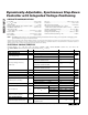
Dynamically-Adjustable, Synchronous Step-Down Controller with Integrated Voltage Positioning (Circuit of Figure 1, V+ = +15V, VCC = VDD = 5V, VPCS = ZMODE = GND = PGND, SKP/SDN = CODE = VCC, VOUT set to 1.5V, TA = 0°C to +85°C, unless otherwise noted. Typical values are at TA = +25°C.
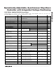
MAX1813 Dynamically-Adjustable, Synchronous Step-Down Controller with Integrated Voltage Positioning ELECTRICAL CHARACTERISTICS (continued) (Circuit of Figure 1, V+ = +15V, VCC = VDD = 5V, VPCS = ZMODE = GND = PGND, SKP/SDN = CODE = VCC, VOUT set to 1.5V, TA = 0°C to +85°C, unless otherwise noted. Typical values are at TA = +25°C.) PARAMETER SYMBOL CONDITIONS MIN TYP MAX UNITS VBST - VLX forced to 5V 1.2 3.5 Ω High state (pull up) 1.3 3.5 Low state (pull down) 0.4 1.0 IDH DH forced to 2.
Dynamically-Adjustable, Synchronous Step-Down Controller with Integrated Voltage Positioning (Circuit of Figure 1, V+ = +15V, VCC = VDD = 5V, VPCS = ZMODE = GND = PGND, SKP/SDN = CODE = VCC, VOUT set to 1.5V, TA = 0°C to +85°C, unless otherwise noted. Typical values are at TA = +25°C.
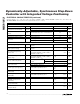
MAX1813 Dynamically-Adjustable, Synchronous Step-Down Controller with Integrated Voltage Positioning ELECTRICAL CHARACTERISTICS (continued) (Circuit of Figure 1, V+ = +15V, VCC = VDD = 5V, VPCS = ZMODE = GND = PGND, SKP/SDN = CODE = VCC, VOUT set to 1.5V, TA = -40°C to +85°C, unless otherwise noted.) (Note 5) PARAMETER SYMBOL Shutdown Supply Current (V+) Reference Voltage CONDITIONS MIN SKP/SDN = GND, VCC = VDD = 0 or 5V VREF REF Fault Lockout Voltage MAX UNITS 5 µA VCC = 4.5V to 5.
Dynamically-Adjustable, Synchronous Step-Down Controller with Integrated Voltage Positioning (Circuit of Figure 1, V+ = +15V, VCC = VDD = 5V, VPCS = ZMODE = GND = PGND, SKP/SDN = CODE = VCC, VOUT set to 1.5V, TA = -40°C to +85°C, unless otherwise noted.) (Note 5) PARAMETER SYMBOL CONDITIONS MIN MAX UNITS 4-Level Logic Input High (VCC) TON (200kHz operation), S0, S1 VCC 0.4 4-Level Logic Input UpperMiddle (Float) TON (300kHz operation), S0, S1 2.8 3.
Typical Operating Characteristics (Circuit from Figure 1, components from Table 2, TA = +25°C, unless otherwise noted.) EFFICIENCY vs. LOAD CURRENT (VOUT = 1.4V) V+ = 4.5V B1: V+ = 7V 100 B1 A1 90 100 MAX1813 toc01 A1: C1 90 B1 A1 D1: V+ = 24V PWM MODE (SKIP = VCC) V+ = 4.5V B2: V+ = 7V C2: V+ = 15V D2: V+ = 24V D1 80 C2 70 D2 60 C2 D2 70 60 0.1 1 10 100 0.1 1 10 90 A1 B1 C1 80 C2 D1 D2 70 1.44 100 PWM MODE SKIP MODE 1.42 1.40 1.38 VBATT = 7V 1.36 1.
Dynamically-Adjustable, Synchronous Step-Down Controller with Integrated Voltage Positioning SWITCHING FREQUENCY vs. TEMPERATURE 380 ON TIME (ns) IOUT = 5A 280 260 360 IOUT = 5A 340 320 IOUT = 1A IOUT = 10A 300 240 IOUT = 20A 280 260 220 -15 10 35 60 -15 10 35 60 85 TEMPERATURE (°C) TEMPERATURE (°C) CURRENT-LIMIT DEVIATION vs. TEMPERATURE NO-LOAD SUPPLY CURRENT vs. BATTERY INPUT VOLTAGE (SKIP MODE) 1.5 ICC + IDD 1.0 SUPPLY CURRENT (mA) VILIM = 2V 1.0 1.2 MAX1813 toc11 2.0 0.
MAX1813 Dynamically-Adjustable, Synchronous Step-Down Controller with Integrated Voltage Positioning Typical Operating Characteristics (continued) (Circuit from Figure 1, components from Table 2, TA = +25°C, unless otherwise noted.) LOAD TRANSIENT (PWM MODE) LOAD TRANSIENT (VOLTAGE POSITIONING DISABLED) LOAD TRANSIENT (SKIP MODE) MAX1813 toc15 MAX1813 toc17 MAX1813 toc16 20A 20A 20A 10A A 0 1.41V B 10A A 0 0 1.41V 1.46V 1.36V 1.36V 1.31V 1.31V 20µs/div A. IOUT = 0.
Dynamically-Adjustable, Synchronous Step-Down Controller with Integrated Voltage Positioning STARTUP WAVEFORM (HEAVY LOAD) STARTUP WAVEFORM (NO LOAD, PWM MODE) MAX1813 toc21 MAX1813 toc22 1.6V 1.6V A 0 5V A 0 5V B 0 1.4V C B 0 1.4V C 0 0 20A 10A D 0 D 0 200µs/div A. VSKP/SDN = 0 TO 1.6V, 2V/div B. PGOOD, 5V/div C. VOUT = 1.4V, ROUT = 63mΩ, 1V/div D. INDUCTOR CURRENT, 20A/div 200µs/div A. VSKP/SDN = 0 TO 1.6V, 2V/div B. PGOOD, 5V/div C. VOUT = 1.4V, NO LOAD, 1V/div D.
Dynamically-Adjustable, Synchronous Step-Down Controller with Integrated Voltage Positioning MAX1813 Pin Description PIN NAME 1 V+ 2 VPCS FUNCTION Battery Voltage Sense Connection. Connect V+ to the input power source. V+ is used only for PWM one-shot timing. DH on-time is inversely proportional to the input voltage over a 2V to 28V range. Current-Sense Input. Connect a current-sense resistor (RSENSE) between VPCS and PGND.
Dynamically-Adjustable, Synchronous Step-Down Controller with Integrated Voltage Positioning PIN NAME 11 REF +2.0V Reference Voltage Output. Bypass to GND with a 0.22µF or greater capacitor. The reference can sink and source ±40µA (min) for external loads. Loading REF degrades FB accuracy according to the REF load regulation error. ILIM Current-Limit Adjustment. The PGND - VPCS current-limit threshold defaults to 50mV if ILIM is tied to VCC.
MAX1813 Dynamically-Adjustable, Synchronous Step-Down Controller with Integrated Voltage Positioning +5V INPUT BIAS SUPPLY C1 1µF BATTERY (VBATT) 7V TO 24V C2 1µF R1 20Ω CIN VDD VCC RGATE 100kΩ ILIM POWER-GOOD INDICATOR V+ BST PGOOD TIME DH CCOMP RTIME 47pF 120kΩ CC MAX1813 CREF 0.22µF L1 0.68µH 1.4V OUTPUT UP TO 22A COUT LX DL REF QL RVPCS 100Ω D2 VPCS CVPCS 1nF RSENSE SUS OPEN S0 OPEN S1 CODE D0 PGND GND ZMODE FB D1 TO VCC QH CBST 0.
Dynamically-Adjustable, Synchronous Step-Down Controller with Integrated Voltage Positioning CIRCUIT 1 (FIGURE 1) COMPONENT Table 2. Component Suppliers MANUFACTURER PHONE [COUNTRY CODE] WEBSITE Output Voltage 0.6V to 1.75V MOSFETs Input Voltage Range 7V to 24V Maximum Load Current 22A Fairchild Semiconductor [1] 888522-5372 www.fairchildsemi.com Inductor 0.68µH Sumida CDEP134H-0R6 or Panasonic ETQP6F0R6BFA International Rectifier [1] 310322-3331 www.irf.
MAX1813 Dynamically-Adjustable, Synchronous Step-Down Controller with Integrated Voltage Positioning VBATT 5V TO 24V REF ILIM V+ TON 5V BIAS VCC 5V BIAS SUPPLY FROM DAC TON COMPUTE BST MAX1813 DH CHIP SUPPLY Q TOFF ONE-SHOT 9R TRIG R LX GND REF S 2V REF TON TRIG ONE-SHOT SET SOFT-START Q R CLR Q Q VPCS ZERO CROSSING VDD CC DL VPCS S Gm 2V REF SKP/SDN REF -12% REF +10% SET Q PGND R CLR Q OVP/UVP DETECT FB SUS PGOOD 5-BIT R-2R DAC S0 DECODER (SEE FIGURE 6) AND SLEW-RAT
Dynamically-Adjustable, Synchronous Step-Down Controller with Integrated Voltage Positioning K(VOUT + 75mV) VIN where K is set by the TON pin-strap connection, and 75mV is an approximation to accommodate for the expected drop across the low-side MOSFET switch and current-sense resistor (Table 3). The on-time one-shot has good accuracy at the operating points specified in the Electrical Characteristics table. On-times at operating points far removed from the conditions specified can vary over a wide range.
MAX1813 Dynamically-Adjustable, Synchronous Step-Down Controller with Integrated Voltage Positioning Table 4. Operating Mode Truth Table SKP/SDN DL MODE COMMENTS GND High Shutdown Micropower shutdown state (ICC = 2µA typ). VCC Switching Normal Operation Automatic switchover from PWM mode to pulse-skipping PFM mode at light loads. Prevents inductor current from recirculating into the input.
Dynamically-Adjustable, Synchronous Step-Down Controller with Integrated Voltage Positioning Current-Limit Circuit (ILIM) The current-limit circuit employs a unique “valley” current-sensing algorithm. If the current-sense signal is above the current-limit threshold, the MAX1813 will not initiate a new cycle (Figure 4). The actual peak current is greater than the current-limit threshold by an amount equal to the inductor ripple current.
MAX1813 Dynamically-Adjustable, Synchronous Step-Down Controller with Integrated Voltage Positioning to select the new 0.600V to 1.750V DAC codes, which are compatible with the IMVP-II specifications. CODE also determines the polarity of ZMODE (Table 7). +5V VBATT BST 5Ω TYP DH LX MAX1813 Figure 5. Reducing the Switching-Node Rise Time Suspend-Mode Operation (S0, S1) When the CPU clock stops, the processor enters suspend mode and requires a lower supply voltage to minimize power consumption.
Dynamically-Adjustable, Synchronous Step-Down Controller with Integrated Voltage Positioning MAX1813 Table 5. Output Voltage vs. DAC Codes D4 D3 D2 D1 D0 0 0 0 0 0 0 0 0 0 0 0 0 0 0 OUTPUT VOLTAGE (V) CODE = 0 CODE = 1 0 2.000 1.750 0 1 1.950 1.700 1 0 1.900 1.650 0 1 1 1.850 1.600 0 1 0 0 1.800 1.550 0 1 0 1 1.750 1.500 0 0 1 1 0 1.700 1.450 0 0 1 1 1 1.650 1.400 0 1 0 0 0 1.600 1.350 0 1 0 0 1 1.550 1.300 0 1 0 1 0 1.500 1.
MAX1813 Dynamically-Adjustable, Synchronous Step-Down Controller with Integrated Voltage Positioning ZMODE MUX D0 D1 D2 D3 D4 D0-D4 DECODER 01 OR 10 OUT IMPEDANCE DECODER IN SUS MUX 0 OUT 00 OR 11 CODE OUT OUT SEL0 SEL1 (FIGURE 7) ZMODE CODE DAC S0/S1 DECODER S0 S1 IN 1 OUT SUS MAX1813 SUS Figure 6. Internal Multiplexers Block Diagram an internal 40kΩ pullup for about 4µs to see if the pin voltage can be forced high (Figure 7).
Dynamically-Adjustable, Synchronous Step-Down Controller with Integrated Voltage Positioning VCC MAX1813 3.0V TO 5.5V 26kΩ 26kΩ 26kΩ 26kΩ 26kΩ D4 100kΩ 100kΩ D3 B-DATA LATCH D2 where ƒSLEW = 150kHz x 120kΩ/RTIME, VOLD is the original output voltage, and VNEW is the new output voltage. See TIME Frequency Accuracy in Electrical Characteristics for ƒSLEW accuracy. The practical range of RTIME is 47kΩ to 470kΩ, corresponding to 2.6µs to 26µs per 25mV step.
MAX1813 Dynamically-Adjustable, Synchronous Step-Down Controller with Integrated Voltage Positioning Output Overvoltage Protection The overvoltage protection circuit is designed to protect the CPU against a shorted high-side MOSFET by drawing high current and activating the battery’s protection circuit. The output voltage is continuously monitored for overvoltage. If the output exceeds the overvoltage threshold, the fault protection is triggered and the circuit shuts down.
Dynamically-Adjustable, Synchronous Step-Down Controller with Integrated Voltage Positioning VSAG = V K L(ILOAD1 -ILOAD2 )2 OUT + t OFF(MIN) VIN (V - V )K 2COUT VOUT IN OUT - t OFF(MIN) V IN where tOFF(MIN) is the minimum off-time (see Electrical Characteristics), and K is from Table 3.
MAX1813 Dynamically-Adjustable, Synchronous Step-Down Controller with Integrated Voltage Positioning ƒ ƒ ESR = SW π where: ƒ ESR = 1 2πRESR COUT For a standard 300kHz application, the ESR zero frequency must be well below 95kHz, preferably below 50kHz. Tantalum, Sanyo POSCAP, and Panasonic SP capacitors in wide-spread use at the time of publication have typical ESR zero frequencies below 30kHz.
Dynamically-Adjustable, Synchronous Step-Down Controller with Integrated Voltage Positioning PD (QH Re sistive) = VIN Generally, a small high-side MOSFET is desired to reduce switching losses at high input voltages. However, the RDS(ON) required to stay within package power-dissipation specifications often limits how small the MOSFET can be. Again, the optimum occurs when the switching losses equal the conduction (RDS(ON)) losses.
MAX1813 Dynamically-Adjustable, Synchronous Step-Down Controller with Integrated Voltage Positioning simple low-pass RC filter with a 100ns time constant (100Ω x 1000pF) sufficiently reduces the noise on the current-sense signal (Figure 8). REF CREF Voltage-Positioning Compensation (CC) Q2 DL RAVPS VPCS CC RVPCS Applications Information CVPCS CCOMP RSENSE MAX1813 PGND GND Figure 8. Voltage-Positioning Block Diagram where D = V OUT /V IN is the regulator’s duty cycle.
Dynamically-Adjustable, Synchronous Step-Down Controller with Integrated Voltage Positioning ESR STEP-DOWN AND STEP-UP (ISTEP x ESR) VOUT CAPACITIVE SAG (dV/dt = IOUT/COUT) RECOVERY from the hot CPU are beneficial. Effective efficiency is defined as the efficiency required of a non-voltagepositioned circuit to equal the total dissipation of a voltage-positioned circuit for a given CPU operating condition.
MAX1813 Dynamically-Adjustable, Synchronous Step-Down Controller with Integrated Voltage Positioning A reasonable minimum value for h is 1.5, but adjusting this up or down allows trade-offs between VSAG, output capacitance, and minimum operating voltage.
Dynamically-Adjustable, Synchronous Step-Down Controller with Integrated Voltage Positioning MAX1813 SUS VCC INV1 R3 30kΩ SUSPEND INV2 C1 10nF R2 80kΩ R1 120kΩ MAX1813 SKP/SDN INV3 ON/OFF tDELAY tDELAY SUSPEND ON/OFF SKIP (2.8V TO 6V) FORCED-PWM (1.4V TO 2.2V) SHUTDOWN (0 TO 0.5V) MAX1813 OPERATING MODE Figure 11. Three-State Operating Mode Control 2.7V TO 5.5V 1kΩ 3.0V TO 5.5V 100kΩ MAX1813 D4 D4 MAX1813 100kΩ D3 D3 ZMODE LOW VID = 01100 1.
MAX1813 Dynamically-Adjustable, Synchronous Step-Down Controller with Integrated Voltage Positioning If the CPU’s VID pins float, the open-circuit pins can present a problem for the MAX1813’s internal mux. The processor’s VID pins can be used for the voltage-mode setting, together with suitable pullup resistors.
Dynamically-Adjustable, Synchronous Step-Down Controller with Integrated Voltage Positioning MAX1813 3.15V TO 5.5V *OPTIONAL 4.7nF 1MΩ 1kΩ 1kΩ 1kΩ 1kΩ 1kΩ MAX1813 D4 100kΩ D3 CPU D2 100kΩ D1 D0 ZMODE CPU VID = 01100 → 1.15V (ZMODE LOW) ZMODE = HIGH = 1.25V ZMODE = LOW = 1.15V ZMODE HIGH VID = 01010 → 1.25V *TO REDUCE QUIESCENT CURRENT, 1kΩ PULLUP RESISTORS CAN BE REPLACED BY 1MΩ RESISTORS WITH 4.7nF CAPACATORS IN PARALLEL. Figure 14.
MAX1813 Dynamically-Adjustable, Synchronous Step-Down Controller with Integrated Voltage Positioning QH DH L1 VOUT LX COUT R4 QL DL MAX1813 RVPCS R5 VPCS CVPCS RSENSE PGND GND FB CFB VOUT = VFB (1 + R4/R5) Figure 16. Adjusting VOUT with a Resistive-Divider Q1 DH L1 VOUT LX MAX1813 COUT Q2 DL RVPCS RFB MAX4634 VPCS R1 CVPCS RSENSE R2 PGND GND R3 R4 REF CREF LOGIC FB CFB ADD0 ADD1 INH CONTROL LOGIC Figure 17.
Dynamically-Adjustable, Synchronous Step-Down Controller with Integrated Voltage Positioning MAX1813 Q1 DH L1 VOUT LX MAX1813 COUT Q2 DL RVPCS RFB VPCS MAX4634 CVPCS RSENSE R5 PGND R6 GND VCC MAX4322 R7 REF R8 CREF LOGIC FB CFB ADD0 ADD1 INH CONTROL LOGIC Figure 18. Adding a Negative Offset Voltage to V+ on the MAX1813, with the same attenuation factor as the output divider. The V+ input has a nominal 600kΩ input impedance, which should be considered when selecting resistor values.
MAX1813 Dynamically-Adjustable, Synchronous Step-Down Controller with Integrated Voltage Positioning about 2-3% at 600kHz when compared to the 300kHz voltage-positioned circuit, primarily due to the high-side MOSFET switching losses. approached in terms of fractions of centimeters, where a single mΩ of excess trace resistance causes a measurable efficiency penalty.
Dynamically-Adjustable, Synchronous Step-Down Controller with Integrated Voltage Positioning plane where sensitive analog components, the GND pin, and VCC bypass capacitor go. The GND plane and PGND plane must meet only at a single point directly beneath the IC. These two planes are then connected to the high-power output ground with a short connection from PGND to the source of the low-side MOSFET (the middle of the star ground). This point must also be very close to the output capacitor ground terminal.
Dynamically-Adjustable, Synchronous Step-Down Controller with Integrated Voltage Positioning QSOP.EPS MAX1813 Package Information Maxim cannot assume responsibility for use of any circuitry other than circuitry entirely embodied in a Maxim product. No circuit patent licenses are implied. Maxim reserves the right to change the circuitry and specifications without notice at any time.