
User Manual
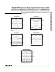
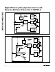

MAX1832–MAX1835
High-Efficiency Step-Up Converters with
Reverse Battery Protection in SOT23-6
2 _______________________________________________________________________________________
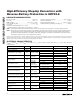
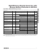
ABSOLUTE MAXIMUM RATINGS
ELECTRICAL CHARACTERISTICS
(V
SHDN
= +1.5V, V
OUT
= +3.3V, V
BATT
= +2V, GND = 0, T
A
= -40°C to +85°C. Typical values are at T
A
= +25°C, unless otherwise
noted.) (Note 3)
Stresses beyond those listed under “Absolute Maximum Ratings” may cause permanent damage to the device. These are stress ratings only, and functional
operation of the device at these or any other conditions beyond those indicated in the operational sections of the specifications is not implied. Exposure to
absolute maximum rating conditions for extended periods may affect device reliability.
BATT, LX to GND.........................................................-6V to +6V
LX to OUT ....................................................................-6V to +1V
SHDN to GND..............................................-6V to (V
OUT
+ 0.3V)
OUT, FB, RST TO GND ............................................-0.3V to +6V
LX Current ................................................................................1A
Continuous Power Dissipation (T
A
= +70°C)
SOT23-6 (derate 9.1mW/°C above +70°C) (Note 1)....727mW
Operating Temperature Range ...........................-40°C to +85°C
Junction Temperature......................................................+150°C
Storage Temperature Range .............................-65°C to +150°C
Lead Temperature (soldering, 10s) (Note 2) ...................+300°C
PARAMETER SYMBOL CONDITIONS MIN TYP MAX UNITS
Output Range V
OUT
MAX1832/MAX1834 2.0 5.5 V
Battery Input Range V
BATT
1.5 5.5 V
T
A
= +25°C 1.22 1.5
Startup Battery Input Voltage V
SU
R
LOAD
= 2.6kΩ
T
A
= -40°C to +85°C 1.24
V
T
A
= +25°C 3.225 3.290 3.355
Output Voltage V
OUT
MAX1833/
MAX1835
T
A
= -40°C to +85°C 3.208 3.372
V
T
A
= +25°C 1.208 1.228 1.248
FB Trip Voltage V
FB
MAX1832/
MAX1834
T
A
= -40°C to +85°C 1.204 1.252
V
T
A
= +25°C 3.5 20
FB Input Bias Current I
FB
MAX1832/
MAX1834,
V
FB
= +1.3V
T
A
= -40°C to +85°C 4.0
nA
T
A
= +25°C 0.4 1.2
N-Channel On-Resistance R
NCH
V
OUT
= +3.3V
I
LX
= 100mA
T
A
= -40°C to +85°C 1.5
Ω
T
A
= +25°C 0.5 1.3
P-Channel On-Resistance R
PCH
V
OUT
= +3.3V
I
LX
= 100mA
T
A
= -40°C to +85°C 1.6
Ω
P-Channel Catch-Diode Voltage
I
LX
= 100mA, PCH off, V
OUT
= +3.5V,
V
FB
= +1.3V
0.73 V
T
A
= +25°C 435 525 615
N-Channel Switch Current Limit I
MAX
V
OUT
= +3.3V
T
A
= -40°C to +85°C 400 650
mA
Switch Maximum On-Time t
ON
3.5 5 6.5 µs
T
A
= +25°C 2 17 34
Synchronous Rectifier Zero-
Crossing Current
V
OUT
= +3.3V
T
A
= -40°C to +85°C0 39
mA
T
A
= +25°C 2.5 7.0
Quiescent Current into OUT
(Note 4)
V
OUT
= +3.5V,
V
FB
= +1.3V
T
A
= -40°C to +85°C 8.0
µA
Shutdown Current into OUT V
OUT
= +3.5V, V
SHDN
= V
FB
= 0V 0.05 1 µA
Note 1: Thermal properties are specified with product mounted on PC board with one square-inch of copper area and still air.
Note 2: This device is constructed using a unique set of packaging techniques that impose a limit on the thermal profile the device
can be exposed to during solder attach and rework. This limit permits only the use of the solder profiles recommended in
the industry-standard specification, IPC/JEDEC J-STD-020A, paragraph 7.6, Table 3 for the IR/VPR and Convection reflow.
Preheating is required. Hand or wave soldering is not allowed.