
User Manual

MAX1832–MAX1835
High-Efficiency Step-Up Converters with
Reverse Battery Protection in SOT23-6
_______________________________________________________________________________________ 9
range to minimize battery drain. Calcuate R4 as follows:
R4 = R3
✕
(V
OFF
/ V
SHDN
- 1)
V
OFF
is the battery voltage at which the part will shut
down and V
SHDN
= 1.228V. Note that input ripple can
sometimes cause false shutdowns. To minimize the effect
of ripple, connect a low-value capacitor (C1) from SHDN
to GND to filter out input noise. Select a C1 value such
that the R4
✕
C1 time constant is above 2ms.
Power-On Reset
The MAX1833/MAX1835 provide a power-on reset out-
put (RST). A 100kΩ to 1MΩ pullup resistor from RST to
OUT provides a logic control signal. This open-drain
output pulls low when the output is 10% below its regu-
lation point. If not used, connect it to GND.
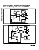
Setting the Output Voltage
The output voltage of the MAX1832/MAX1834 is
adjustable from +2V to +5.5V, using external resistors
R1 and R2 (Figure 1b). Since FB leakage is 20nA
(max), select feedback resistor R1 to be 100kΩ to
1MΩ. Calculate R2 as follows:
where V
FB
= 1.228V.
Inductor Selection
The control scheme of the MAX1832–MAX1835 permits
flexibility in choosing an inductor. A 10µH inductor per-
forms well for most applications, but values from 4.7µH
to 100µH may also be used. Small inductance values
typically offer smaller physical size. Large inductance
values minimize output ripple but reduce output power.
Output power is reduced when the inductance is large
enough to prevent the maximum current limit (525mA)
from being reached before the maximum on-time (5µs)
expires.
For maximum output current, choose L such that:
where R
IND
is the inductor series resistance, and R
NCH
is the R
DS(ON)
of the N-channel MOSFET (0.4Ω typ).
Capacitor Selection
Choose an output capacitor to achieve the desired out-
put ripple percentage.
where r is the desired output ripple in %. A 10µF ceramic
capacitor is a good starting value. The input capacitor
reduces the peak current drawn from the battery and
can be the same value as the input capacitor. A larger
input capacitor can be used to further reduce ripple and
improve efficiency.
PC Board Layout and Grounding
Careful printed circuit layout is important for minimizing
ground bounce and noise. Keep the IC’s GND pin and
the ground leads of the input and output filter capaci-
tors less than 0.2in (5mm) apart. In addition, keep all
connections to the FB and LX pins as short as possible.
In particular, when using external feedback resistors,
C
LA
rV
OUT
OUT
>
××
×
05 0525
2
2
..
%
I
A
V
A
RR
V
OUT MAX
BATT MIN NCH IND
OUT
()
()
.
.
=
×
−+
()
0 525
2
0 525
2
Vs
A
L
Vs
A
BATT MAX BATT MIN() ()
..
1
0 525
5
0 525
µµ
()
<<
()
RR
V
V
OUT
FB
21 1=−
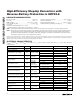
MANUFACTURER INDUCTOR PHONE
Coilcraft
DS1608C-103
DO1606T-103
847-639-6400
Sumida
CDRH4D18-100
CR43-100
847-956-0666
Murata LQH4N100K 814-237-1431
Table 1. Suggested Inductors and
Suppliers
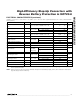
VALUE
(µF)
DESCRIPTION
MANU-
FACTURER
PHONE
594/595 D-
series tantalum
Sprague 603-224-1961
4.7 to
47
TAJ, TPS-
series tantalum
AVX 803-946-0690
4.7 to
10
X7R ceramic TDK 847-390-4373
4.7 to
22
X7R ceramic Taiyo Yuden 408-573-4150
Table 2. Suggested Surface-Mount
Capacitors and Manufacturers