
User guide


MAX186/MAX188
Internal and External Clock Modes
The MAX186/MAX188 may use either an external serial
clock or the internal clock to perform the
successive-approximation conversion. In both clock
modes, the external clock shifts data in and out of the
MAX186/MAX188. The T/H acquires the input signal as
the last three bits of the control byte are clocked into
DIN. Bits PD1 and PD0 of the control byte program the
clock mode. Figures 7 through 10 show the timing
characteristics common to both modes.
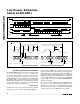
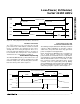
External Clock
In external clock mode, the external clock not only shifts
data in and out, it also drives the analog-to-digital con-
version steps. SSTRB pulses high for one clock period
after the last bit of the control byte. Successive-approxi-
mation bit decisions are made and appear at DOUT on
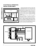
each of the next 12 SCLK falling edges (see Figure 6).
SSTRB and DOUT go into a high-impedance state when
CS goes high; after the next CS falling edge, SSTRB will
output a logic low. Figure 8 shows the SSTRB timing in
external clock mode.
The conversion must complete in some minimum time, or
else droop on the sample-and-hold capacitors may
degrade conversion results. Use internal clock mode if the
clock period exceeds 10µs, or if serial-clock interruptions
could cause the conversion interval to exceed 120µs.
Low-Power, 8-Channel,
Serial 12-Bit ADCs
12 ______________________________________________________________________________________
SSTRB
CS
SCLK
DIN
DOUT
14 8 12 16 20 24
START
SEL2 SEL1 SEL0
UNI/
BIP
SCL/
DIFF
PD1 PD0
B11
MSB
B10 B9 B8 B7 B6 B5 B4 B3 B2 B1
B0
LSB
ACQUISITION
1.5µs (CLK = 2MHz)
IDLE
FILLED WITH
ZEROS
IDLE
CONVERSION
t
ACQ
A/D STATE
RB1
RB2
RB3
• • •
• • •
• • •
• • •
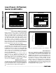
CS
SCLK
DIN
DOUT
t
CSH
t
CSS
t
CL
t
DS
t
DH
t
DV
t
CH
t
DO
t
TR
t
CSH
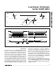
Figure 6. 24-Bit External Clock Mode Conversion Timing (SPI, QSPI and Microwire Compatible)
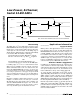
Figure 7. Detailed Serial-Interface Timing