
User guide


MAX186/MAX188
Lowest Power at Higher Throughputs
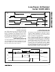
Figure 14b shows the power consumption with
external-reference compensation in fast power-down,
with one and eight channels converted. The external
4.7µF compensation requires a 50µs wait after power-up,
accomplished by 75 idle clocks after a dummy conver-
sion. This circuit combines fast multi-channel conversion
with lowest power consumption possible. Full
power-down mode may provide increased power sav-
ings in applications where the MAX186/MAX188 are
inactive for long periods of time, but where intermittent
bursts of high-speed conversions are required.
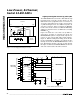
External and Internal References
The MAX186 can be used with an internal or external
reference, whereas an external reference is required for
the MAX188. Diode D1 shown in the
Typical Operating
Circuit
ensures correct start-up. Any standard signal
diode can be used. For both parts, an external refer-
ence can either be connected directly at the VREF ter-
minal or at the REFADJ pin.
An internal buffer is designed to provide 4.096V at
VREF for both the MAX186 and MAX188. The
MAX186’s internally trimmed 2.46V reference is
buffered with a gain of 1.678. The MAX188's buffer is
trimmed with a buffer gain of 1.638 to scale an external
2.5V reference at REFADJ to 4.096V at VREF.
MAX186 Internal Reference
The full-scale range of the MAX186 with internal reference
is 4.096V with unipolar inputs, and ±2.048V with bipolar
inputs. The internal reference voltage is adjustable to
±1.5% with the Reference-Adjust Circuit of Figure 17.
External Reference
With both the MAX186 and MAX188, an external refer-
ence can be placed at either the input (REFADJ) or the
output (VREF) of the internal buffer amplifier. The
REFADJ input impedance is typically 20kΩ for the
MAX186 and higher than 100kΩ for the MAX188, where
the internal reference is omitted. At VREF, the input
impedance is a minimum of 12kΩ for DC currents.
During conversion, an external reference at VREF must
be able to deliver up to 350µA DC load current and have
an output impedance of 10Ω or less. If the reference has
higher output impedance or is noisy, bypass it close to
the VREF pin with a 4.7µF capacitor.
Low-Power, 8-Channel,
Serial 12-Bit ADCs
18 ______________________________________________________________________________________
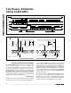
1000
1
0 100 300 500
MAX186
FULL POWER-DOWN
10
100
MAX186-14A
CONVERSIONS PER CHANNEL PER SECOND
200 400
2ms FASTPD WAIT
400kHz EXTERNAL CLOCK
INTERNAL COMPENSATION
50 150 250 350 450
8 CHANNELS
1 CHANNEL
AVG. SUPPLY CURRENT (µA)
10,000
10
0
MAX186/MAX188
FAST POWER-DOWN
100
1000
CONVERSIONS PER CHANNEL PER SECOND
2k
8 CHANNELS
1 CHANNEL
4k 6k 8k 10k 12k 14k 16k 18k
2MHz EXTERNAL CLOCK
EXTERNAL COMPENSATION
50µs WAIT
AVG. SUPPLY CURRENT (µA)
Figure 14a. MAX186 Supply Current vs. Sample Rate/Second,
FULLPD, 400kHz Clock
Figure 14b. MAX186/MAX188 Supply Current vs. Sample
Rate/Second, FASTPD, 2MHz Clock
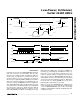
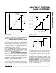
3.0
2.5
2.0
1.5
1.0
0.5
0
0.0001 0.001 0.01 0.1 1 10
TIME IN SHUTDOWN (sec)
POWER-UP DELAY (ms)
Figure 14c. Typical Power-Up Delay vs. Time in Shutdown