
User guide


MAX186/MAX188
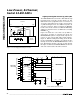
High-Speed Digital Interfacing with QSPI
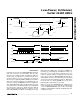
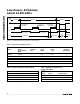
The MAX186/MAX188 can interface with QSPI at high
throughput rates using the circuit in Figure 19. This
QSPI circuit can be programmed to do a conversion on
each of the eight channels. The result is stored in mem-
ory without taxing the CPU since QSPI incorporates its
own micro-sequencer. Figure 19 depicts the MAX186,
but the same circuit could be used with the MAX188 by
adding an external reference to VREF and connecting
REFADJ to V
DD
.
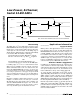
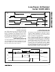
Figure 20 details the code that sets up QSPI for
autonomous operation. In external clock mode, the
MAX186/MAX188 perform a single-ended, unipolar con-
version on each of their eight analog input channels.
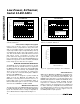
Figure 21, QSPI Assembly-Code Timing, shows the tim-
ing associated with the assembly code of Figure 20. The
first byte clocked into the MAX186/MAX188 is the control
byte, which triggers the first conversion on CH0. The last
two bytes clocked into the MAX186/MAX188 are all zero
and clock out the results of the CH7 conversion.
Low-Power, 8-Channel,
Serial 12-Bit ADCs
20 ______________________________________________________________________________________
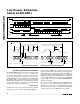
+5V
-5V
GND
SUPPLIES
DGND+5VDGNDV
SS
AGNDV
DD
DIGITAL
CIRCUITRY
MAX186/MAX188
R* = 10Ω
* OPTIONAL
Figure 18. Power-Supply Grounding Connection
20
19
18
17
16
15
14
13
12
11
2
3
4
5
6
7
8
9
10
MAX186
CH0
CH1
CH2
CH3
CH4
CH5
CH6
CH7
V
SS
SHDN
V
DD
SCLK
CS
DIN
SSTRB
DOUT
DGND
AGND
REFADJ
VREF
V
DDI
, V
DDE
, V
DDSYN
, V
STBY
SCK
PCS0
MOSI
MISO
* CLOCK CONNECTIONS NOT SHOWN
V
SSI
VSSE
MC68HC16
0.1µF 4.7µF
0.01µF
0.1µF
4.7µF
ANALOG
INPUTS
+5V
+
1
Figure 19. MAX186 QSPI Connection