
User guide


MAX186/MAX188
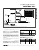
_______________Detailed Description
The MAX186/MAX188 use a successive-approximation
conversion technique and input track/hold (T/H) circuit-
ry to convert an analog signal to a 12-bit digital output.
A flexible serial interface provides easy interface to
microprocessors. No external hold capacitors are
required. Figure 3 shows the block diagram for the
MAX186/MAX188.
Pseudo-Differential Input
The sampling architecture of the ADC’s analog com-
parator is illustrated in the Equivalent Input Circuit
(Figure 4). In single-ended mode, IN+ is internally
switched to CH0-CH7 and IN- is switched to AGND. In
differential mode, IN+ and IN- are selected from pairs
of CH0/CH1, CH2/CH3, CH4/CH5 and CH6/CH7.
Configure the channels with Table 3 and Table 4.
In differential mode, IN- and IN+ are internally switched
to either one of the analog inputs. This configuration is
pseudo-differential to the effect that only the signal at
IN+ is sampled. The return side (IN-) must remain sta-
ble within ±0.5LSB (±0.1LSB for best results) with
respect to AGND during a conversion. Accomplish this
by connecting a 0.1µF capacitor from AIN- (the select-
ed analog input, respectively) to AGND.
During the acquisition interval, the channel selected as
the positive input (IN+) charges capacitor C
HOLD
. The
acquisition interval spans three SCLK cycles and ends
on the falling SCLK edge after the last bit of the input
control word has been entered. At the end of the acqui-
sition interval, the T/H switch opens, retaining charge
on C
HOLD
as a sample of the signal at IN+.
The conversion interval begins with the input multiplex-
er switching C
HOLD
from the positive input (IN+) to the
negative input (IN-). In single-ended mode, IN- is sim-
ply AGND. This unbalances node ZERO at the input of
the comparator. The capacitive DAC adjusts during the
remainder of the conversion cycle to restore node
ZERO to 0V within the limits of 12-bit resolution. This
action is equivalent to transferring a charge of 16pF x
[(V
IN
+) - (V
IN
-)] from C
HOLD
to the binary-weighted
capacitive DAC, which in turn forms a digital represen-
tation of the analog input signal.
Track/Hold
The T/H enters its tracking mode on the falling clock
edge after the fifth bit of the 8-bit control word has been
shifted in. The T/H enters its hold mode on the falling
clock edge after the eighth bit of the control word has
been shifted in. If the converter is set up for
single-ended inputs, IN- is connected to AGND, and
the converter samples the “+” input. If the converter is
set up for differential inputs, IN- connects to the “-”
input, and the difference of
|IN+ - IN-| is sampled. At
the end of the conversion, the positive input connects
back to IN+, and C
HOLD
charges to the input signal.
The time required for the T/H to acquire an input signal
is a function of how quickly its input capacitance is
charged. If the input signal’s source impedance is high,
the acquisition time lengthens and more time must be
allowed between conversions. Acquisition time is cal-
culated by:
t
AZ
= 9 x (R
S
+ R
IN
) x 16pF,
where R
IN
= 5kΩ, R
S
= the source impedance of the
input signal, and t
AZ
is never less than 1.5µs. Note that
source impedances below 5kΩ do not significantly
affect the AC performance of the ADC. Higher source
impedances can be used if an input capacitor is con-
nected to the analog inputs, as shown in Figure 5. Note
that the input capacitor forms an RC filter with the input
source impedance, limiting the ADC’s signal bandwidth.
Input Bandwidth
The ADC’s input tracking circuitry has a 4.5MHz
small-signal bandwidth, so it is possible to digitize
high-speed transient events and measure periodic sig-
nals with bandwidths exceeding the ADC’s sampling
rate by using undersampling techniques. To avoid
high-frequency signals being aliased into the frequency
band of interest, anti-alias filtering is recommended.
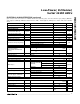
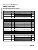
Low-Power, 8-Channel,
Serial 12-Bit ADCs
8 _______________________________________________________________________________________
CH0
CH1
CH2
CH3
CH4
CH5
CH6
CH7
AGND
C
SWITCH
TRACK
T/H
SWITCH
10k
R
S
C
HOLD
HOLD
12-BIT CAPACITIVE DAC
VREF
ZERO
COMPARATOR
–
+
16pF
SINGLE-ENDED MODE: IN+ = CHO-CH7, IN– = AGND.
DIFFERENTIAL MODE: IN+ AND IN– SELECTED FROM PAIRS OF
CH0/CH1, CH2/CH3, CH4/CH5, CH6/CH7.
AT THE SAMPLING INSTANT,
THE MUX INPUT SWITCHES
FROM THE SELECTED IN+
CHANNEL TO THE SELECTED
IN– CHANNEL.
INPUT
MUX
Figure 4. Equivalent Input Circuit