
Owner's manual
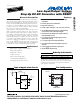

MAX1947
Low Input/Output Voltage
Step-Up DC-DC Converter with
RESET
2 _______________________________________________________________________________________
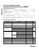
ABSOLUTE MAXIMUM RATINGS
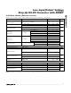
ELECTRICAL CHARACTERISTICS
(V
BATT
= 1.5V, T
A
= -40°C to +85°C, unless otherwise noted. Typical values are at T
A
= +25°C.) (Note 2)
Stresses beyond those listed under “Absolute Maximum Ratings” may cause permanent damage to the device. These are stress ratings only, and functional
operation of the device at these or any other conditions beyond those indicated in the operational sections of the specifications is not implied. Exposure to
absolute maximum rating conditions for extended periods may affect device reliability.
Note 1: LX has internal clamp diodes to PGND and OUT. Applications that forward bias these diodes should take care not to exceed the
IC’s package power-dissipation limits.
BATT, OUT, SHDN to GND ...................................-0.3V to +4.0V
RESET to GND..........................................-0.3V to (V
OUT
+ 0.3V)
PGND to GND .......................................................-0.3V to +0.3V
Switch Current (I
LX
, I
OUT
, I
PGND
) (Note 1) .................-1A to +1A
Continuous Power Dissipation (T
A
= +70°C)
8-Pin TDFN (derate 24.4mW/°C
above +70°C)..........................................................1951.2mW
Operating Temperature Range ...........................-40°C to +85°C
Junction Temperature......................................................+150°C
Storage Temperature Range .............................-65°C to +150°C
Lead Temperature (soldering, 10s) .................................+300°C
PARAMETER CONDITIONS MIN TYP MAX UNITS
Minimum Startup Voltage R
LOAD
= 1kΩ, T
A
= +25°C 0.8 0.95 V
Startup-Voltage Temperature
Coefficient
-2.1 mV/°C
Maximum Input Operating
Voltage
(Note 3) 3.6 V
Minimum Input Operating Voltage 0.7 V
MAX1947ETA18, I
LOAD
= 40mA 1.74 1.8 1.86
MAX1947ETA25, I
LOAD
= 32mA 2.42 2.5 2.58
MAX1947ETA30, I
LOAD
= 25mA 2.9 3.0 3.1
Output Voltage
MAX1947ETA33, I
LOAD
= 25mA 3.2 3.3 3.4
V
Load Regulation No load to full load 1.2 %
MAX1947ETA18 160 273
MAX1947ETA25 130 214
MAX1947ETA30 100 185
V
BATT
= 1V
MAX1947ETA33 100 169
MAX1947ETA25 240 380
MAX1947ETA30 200 361
Full-Load Output Current
V
BATT
= 1.8V
MAX1947ETA33 200 329
mA
Supply Current into BATT No switching 2 4 µA
Supply Current into OUT No switching 70 110 µA
LX Switch Maximum On-Time 0.7 1 1.3 µs
LX Switch Minimum Off-Time 0.2 0.25 0.3 µs
Maximum On-Time to Minimum
Off-Time Ratio
3.6 4 4.6
Frequency in Startup 650 kHz