
Instruction Manual


_______________________________________________________________________________________ 3
MAX5042/MAX5043
Two-Switch Power ICs with Integrated
Power MOSFETs and Hot-Swap Controller
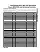
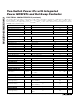
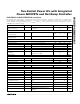
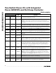
ELECTRICAL CHARACTERISTICS
(V
POSINPWM
= 20V to 76V, V
REG15
= 18V, C
REG15
= 4.7µF, C
REG9
= 1µF, C
REG5
= 1µF, R
RCOSC
= 24kΩ, C
RCOSC
= 100pF, C
BST
=
0.22µF, R
DRVDEL
= 10kΩ, C
DRVDEL
= 0.22µF, V
CSS
= V
CSP
= V
CSN
= V
RAMP
= V
PWMNEG
= V
NEGIN
= 0, T
A
= -40°C to +125°C,
unless otherwise noted. Typical values are at V
POSINPWM
= 48V, T
A
= +25°C, unless otherwise noted. All voltages are referred to
PWMNEG, unless otherwise noted.)
PARAMETER
SYMBOL
CONDITIONS
MIN
TYP
MAX
UNITS
Input Supply Range
V
POSINPWM
20 76 V
REG15 REGULATOR
REG15 Output Voltage Range
V
REG15
V
POSINPWM
= 20V to 76V
13.0 16.6
V
REG15 Output Voltage Load
Regulation
V
POSINPWM
= 20V, I
REG15
= 0 to 80mA 1.5 V
REG15 Output Current Inferred from load regulation test 80 mA
REG15 Current Limit REG15 shorted to PWMNEG with 10Ω
140
mA
REG15 Overdrive Voltage 18 40 V
REG9 REGULATOR
REG9 Output Voltage Range V
REG15
= 18V to 40V 8.3
10.1
V
REG9 Output Voltage Load
Regulation
I
REG9
= 0 to 40mA
0.35
V
REG9 Output Current Inferred from load regulation test 40 mA
REG9 Current Limit REG9 shorted to PWMNEG with 10Ω
100
mA
REG5 REGULATOR
REG5 Output Voltage Range V
REG15
= 18V to 40V 4.5 5.5 V
REG5 Output Voltage Load
Regulation
I
REG5
= 0 to 20mA
0.35
V
REG5 Output Current Inferred from load regulation test 20 mA
REG5 Current Limit REG5 shorted to PWMNEG with 10Ω 40 mA
PWM COMPARATOR
Common-Mode Range
V
CM-PWM
0 5.5 V
Input Offset Voltage 10 mV
Input Bias Current
-2.5 +2.5
µA
Propagation Delay 50mV overdrive, 0 ≤ V
CM-PWM
≤ 5.5V 70 ns
RCOSC OSCILLATOR
PWM Period
t
OSC-PWM
3.9 µs
Maximum Duty Cycle 47 %
Maximum RCOSC Frequency f
RCOSC
1.2
MHz
RCOSC Peak Trip Level V
TH
2.55
V
RCOSC Valley Trip Level 0.2 V
RCOSC Input Bias Current
-0.3
µA
RCOSC Discharge MOSFET
R
DS(ON)
Sinking 10mA 60
120
Ω
RCOSC Discharge Pulse Width 50 ns
SYNC High Level 3.5 V
SYNC Low Level 0.8 V