
Owner manual


MAX5099
Dual, 2.2MHz, Automotive Synchronous Buck
Converter with 80V Load-Dump Protection
2 _______________________________________________________________________________________
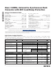
ABSOLUTE MAXIMUM RATINGS
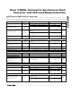
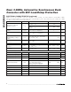
ELECTRICAL CHARACTERISTICS
(VDRV = V
L
, V+ = V
L
= IN_HIGH = 5.2V or V+ = IN_HIGH = 5.2V to 19V, EN_ = V
L
, SYNC = GND, I
VL
= 0mA, PGND = SGND,
C
BYPASS
= 0.22μF (low ESR), C
VL
= 4.7μF (ceramic), C
V+
= 1μF (low ESR), C
IN_HIGH
= 1μF (ceramic), R
IN_HIGH
= 3.9kΩ, R
OSC
= 10kΩ,
T
J
= -40°C to +125°C, unless otherwise noted.) (Note 2)
Stresses beyond those listed under “Absolute Maximum Ratings” may cause permanent damage to the device. These are stress ratings only, and functional
operation of the device at these or any other conditions beyond those indicated in the operational sections of the specifications is not implied. Exposure to
absolute maximum rating conditions for extended periods may affect device reliability.
Note 1: Package thermal resistances were obtained using the method described in JEDEC specifications. For detailed information
on package thermal considerations refer to www.maxim-ic.com/thermal-tutorial
.
V+ to SGND............................................................-0.3V to +25V
V+ to IN_HIGH...........................................................-19V to +6V
IN_HIGH to SGND ..................................................-0.3V to +19V
IN_HIGH Maximum Input Current .......................................60mA
BYPASS to SGND..................................................-0.3V to +2.5V
GATE to V+.............................................................-0.3V to +12V
GATE to SGND .......................................................-0.3V to +36V
SGND to PGND .....................................................-0.3V to +0.3V
V
L
to SGND..................-0.3V to the Lower of +6V or (V+ + 0.3V)
VDRV to SGND .........................................................-0.3V to +6V
BST1/VDD1, BST2/VDD2, DRAIN_,
PGOOD_ to SGND ..............................................-0.3V to +30V
ON/OFF to SGND ...............................-0.3V to (IN_HIGH + 0.3V)
BST1/VDD1 to SOURCE1,
BST2/VDD2 to SOURCE2......................................-0.3V to +6V
SOURCE_ to SGND................................................-0.6V to +25V
EN_ to SGND............................................................-0.3V to +6V
OSC, FSEL_1, COMP_, SYNC,
FB_ to SGND..............................................-0.3V to (V
L
+ 0.3V)
DL_ to PGND ...........................................-0.3V to (VDRV + 0.3V)
SOURCE1, DRAIN1 Peak Current ..............................5A for 1ms
SOURCE2, DRAIN2 Peak Current ..............................3A for 1ms
V
L
, BYPASS to
SGND Short Circuit ................... Continuous, Internally Limited
Continuous Power Dissipation (T
A
= +70°C)
32-Pin TQFN-EP (derate 34.5mW/°C above +70°C)..2759mW
Package Junction-to-Ambient
Thermal Resistance (θ
JA
) (Note 1).............................29.0°C/W
Package Junction-to-Case
Thermal Resistance (θ
JC
) (Note 1) ..............................1.7°C/W
Operating Temperature Range .........................-40°C to +125°C
Storage Temperature Range ............................-65°C to +150°C
Junction Temperature......................................................+150°C
Lead Temperature (soldering, 10s) ................................+300°C
PARAMETER SYMBOL CONDITIONS MIN TYP MAX UNITS
SYSTEM SPECIFICATIONS
V+ = IN_HIGH 5.2 19
Input Voltage Range V+
V
L
= V+ = IN_HIGH, Figure 6 (Note 3) 4.5 5.5
V
V+ Operating Supply Current I
Q
V
L
unloaded, no switching, V
FB_
= 1V 4.2 6.0 mA
V+ Standby Supply Current I
V+STBY
V
EN_
= 0V, PGOOD_ unconnected,
V+ = V
IN_HIGH
= 14V
0.75 1.1 mA
V+ = V
L
= 5.2V 86
V+ = 12V 85
Efficiency η
V
OUT1
= 5V at 1.5A,
V
OUT2
= 3.3V at 0.75A,
f
SW
= 300kHz
V+ = 16V 85
%
OVERVOLTAGE PROTECTOR
IN_HIGH Clamp Voltage IN_HIGH I
SINK
= 10mA 19 20 21 V
IN_HIGH Clamp Load
Regulation
1mA < I
SINK
< 50mA 160 mV
IN_HIGH Supply Current I
IN_HIGH
V
EN_
= V
PGOOD_
= V
GATE
= 0V,
V
IN_HIGH
= V
ON/OFF
= 14V
270 600 μA
IN_HIGH Standby Supply
Current
I
IN_HIGHSTBY
V
ON/OFF
= 0V , V
PGOOD_
= V + =
unconnected, V
IN_HIGH
= 14V
79μA
V+ to IN_HIGH Overvoltage
Clamp
V
OV
V
OV
= V+ - V
IN_HIGH
, I
GATE
= -1mA 1.20 1.85 2.50 V