
Owner manual


MAX5132/MAX5133
+5V/+3V, 13-Bit, Serial, Force/Sense DACs
with 10ppm/°C Internal Reference
10 ______________________________________________________________________________________
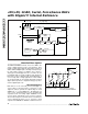
_______________Detailed Description
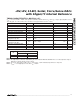
The MAX5132/MAX513313-bit, force/sense DACs are
easily configured with a 3-wire serial interface. They
include a 16-bit data-in/data-out shift register and have a
double-buffered digital input consisting of an input regis-
ter and a DAC register. In addition, these devices
employ precision bandgap references, as well as an out-
put amplifier with accessible feedback and output pins
that can be used for setting the gain externally (Figure 1)
or for forcing and sensing applications. These DACs
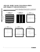
are designed with an inverted R-2R ladder network
(Figure 2) that produces a weighted voltage proportion-
al to the digital input code.
Internal Reference
Both devices use an on-board precision bandgap ref-
erence with a low temperature coefficient of only
10ppm/°C (max) to generate an output voltage of +2.5V
(MAX5132) or +1.25V (MAX5133). The REF pin can
source up to 100µA and may become unstable with
capacitive loads exceeding 100pF. REFADJ can be
used for minor adjustments to the reference voltage.
The circuits in Figures 3a and 3b achieve a nominal ref-
erence adjustment range of ±1%. Connect a 33nF
capacitor from REFADJ to AGND to establish low-noise
MAX5132
MAX5133
SR
CONTROL
16-BIT
SHIFT REGISTER
DECODE
CONTROL
INPUT
REGISTER
BANDGAP
REFERENCE
REFERENCE
BUFFER
DAC
REGISTER
DAC
2X
(X1)
DOUT
UPO
OUT
FB
13
4k
1.25V
AGND DGNDV
DDDIN SCLKCS
2.5V (1.25V)
LOGIC
OUTPUT
CLR
PDL
PD
RSTVAL
REFADJ
( ) FOR MAX5133 ONLY.
REF
Figure 1. Simplified Functional Diagram
OUT
FB
SHOWN FOR ALL 1s ON DAC
D0 D10 D11
D12
*INTERNAL REFERENCE: 2.5V (MAX5132),
1.25V (MAX5133); OR EXTERNAL REFERENCE
2R
2R 2R 2R 2R
RRR
REF*
AGND
Figure 2. Simplified Inverted R-2R DAC Structure